SNOSD56 June 2017 LF412-N-MIL
PRODUCTION DATA.
- 1 Features
- 2 Applications
- 3 Description
- 4 Revision History
- 5 Pin Configuration and Functions
- 6 Specifications
- 7 Detailed Description
- 8 Application and Implementation
- 9 Power Supply Recommendations
- 10Layout
- 11Device and Documentation Support
- 12Mechanical, Packaging, and Orderable Information
Package Options
Mechanical Data (Package|Pins)
- LMC|8
Thermal pad, mechanical data (Package|Pins)
Orderable Information
10 Layout
10.1 Layout Guidelines
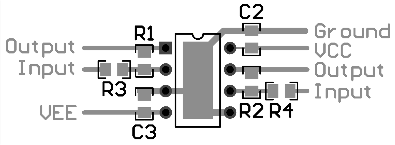
As with most amplifiers, care should be taken with lead dress, component placement and supply decoupling in order to ensure stability. For example, resistors from the output to an input should be placed with the body close to the input to minimize “pick-up” and maximize the frequency of the feedback pole by minimizing the capacitance from the input to ground.
10.2 Layout Example
 Figure 31. LF412-N-MIL Layout