SNVS729F September 2011 – August 2014 LM10506
PRODUCTION DATA.
- 1 Features
- 2 Applications
- 3 Description
- 4 Revision History
- 5 Device Comparison Table
- 6 Pin Configuration and Functions
-
7 Specifications
- 7.1 Absolute Maximum Ratings
- 7.2 Handling Ratings
- 7.3 Recommended Operating Conditions
- 7.4 Thermal Information
- 7.5 General Electrical Characteristics
- 7.6 Buck 1 Electrical Characteristics
- 7.7 Buck 2 Electrical Characteristics
- 7.8 Buck 3 Electrical Characteristics
- 7.9 LDO Electrical Characteristics
- 7.10 Comparators Electrical Characteristics
- 7.11 Typical Characteristics
-
8 Detailed Description
- 8.1 Functional Block Diagram
- 8.2 Feature Description
- 8.3 Device Functional Modes
- 8.4 Programming
-
9 Application and Implementation
- 9.1 Application Information
- 9.2 Typical Application
- 10Power Supply Recommendations
- 11Layout
- 12Device and Documentation Support
- 13Mechanical, Packaging, and Orderable Information
Package Options
Mechanical Data (Package|Pins)
- YFR|34
Thermal pad, mechanical data (Package|Pins)
Orderable Information
8 Detailed Description
The LM10506 is a highly efficient and integrated Power Management Unit for Systems-on-a-Chip (SoCs), ASICs, and processors. It operates cooperatively and communicates with processors over an SPI interface with output Voltage programmability and Standby Mode.
The device incorporates three high-efficiency synchronous buck regulators and one LDO that deliver four output voltages from a single power source. The device also includes a SPI-programmable Comparator Block that provides an interrupt output signal.
8.1 Functional Block Diagram
8.2 Feature Description
8.2.1 Buck Regulators Operation
A buck converter contains a control block, a switching PFET connected between input and output, a synchronous rectifying NFET connected between the output and ground and a feedback path. The following figure shows the block diagram of each of the three buck regulators integrated in the device.
 Figure 18. Buck Functional Diagram
During the first portion of each switching cycle, the control block turns on the internal PFET switch. This allows current to flow from the input through the inductor to the output filter capacitor and load. The inductor limits the current to a ramp with a slope of (VIN – VOUT)/L by storing energy in a magnetic field. During the second portion of each cycle, the control block turns the PFET switch off, blocking current flow from the input, and then turns the NFET synchronous rectifier on. The inductor draws current from ground through the NFET to the output filter capacitor and load, which ramps the inductor current down with a slope of (–VOUT)/L.
The output filter stores charge when the inductor current is high, and releases it when low, smoothing the voltage across the load. The output voltage is regulated by modulating the PFET switch on time to control the average current sent to the load. The effect is identical to sending a duty-cycle modulated rectangular wave formed by the switch and synchronous rectifier at the SW pin to a low-pass filter formed by the inductor and output filter capacitor. The output voltage is equal to the average voltage at the SW pin.
8.2.1.1 Buck Regulators Description
The LM10506 incorporates three high-efficiency synchronous switching buck regulators that deliver various voltages from a single DC input voltage. They include many advanced features to achieve excellent voltage regulation, high efficiency and fast transient response time. The bucks feature voltage mode architecture with synchronous rectification.
Each of the switching regulators is specially designed for high-efficiency operation throughout the load range. With a 2MHz typical switching frequency, the external L- C filter can be small and still provide very low output voltage ripple. The bucks are internally compensated to be stable with the recommended external inductors and capacitors as detailed in the application diagram. Synchronous rectification yields high efficiency for low voltage and high output currents.
All bucks can operate up to a 100% duty cycle allowing for the lowest possible input voltage that still maintains the regulation of the output. The lowest input to output dropout voltage is achieved by keeping the PMOS switch on.
Additional features include soft-start, undervoltage lockout, bypass, and current and thermal overload protection. To reduce the input current ripple, the device employs a control circuit that operates the 3 bucks at 120° phase. These bucks are nearly identical in performance and mode of operation. They can operate in FPWM (forced PWM) or automatic mode (PWM/PFM).
8.2.1.2 PWM Operation
During PWM operation the converter operates as a voltage-mode controller with input voltage feed forward. This allows the converter to achieve excellent load and line regulation. The DC gain of the power stage is proportional to the input voltage. To eliminate this dependence, a feed forward voltage inversely proportional to the input voltage is introduced.
In Forced PWM Mode the bucks always operate in PWM mode regardless of the output current.
In Automatic Mode, if the output current is less than 70 mA (typ.), the bucks automatically transition into PFM (Pulse Frequency Modulation) operation to reduce the current consumption. At higher than 100 mA (typ.) they operate in PWM mode. This increases the efficiency at lower output currents. The 30 mA (typ.) hysteresis is designed in for stable Mode transition.
While in PWM mode, the output voltage is regulated by switching at a constant frequency and then modulating the energy per cycle to control power to the load. At the beginning of each clock cycle the PFET switch is turned on, and the inductor current ramps up until the comparator trips and the control logic turns off the switch. The current limit comparator can also turn off the switch in case the current limit of the PFET is exceeded. In this case the NFET switch is turned on and the inductor current ramps down. The next cycle is initiated by the clock turning off the NFET and turning on the PFET.
 Figure 19. PFM vs PWM Operation
8.2.1.3 PFM Operation (Bucks 1, 2 & 3)
At very light loads, Bucks 1, 2, and Buck 3 enter PFM mode and operate with reduced switching frequency and supply current to maintain high efficiency.
Bucks 1, 2, and 3 will automatically transition into PFM mode when either of two conditions occurs for a duration of 32 or more clock cycles:
- The inductor current becomes discontinuous, or
- The peak PMOS switch current drops below the IMODE level.
During PFM operation, the converter positions the output voltage slightly higher than the nominal output voltage during PWM operation, allowing additional headroom for voltage drop during a load transient from light to heavy load. The PFM comparators sense the output voltage via the feedback pin and control the switching of the output FETs such that the output voltage ramps between 0.8% and 1.6% (typical) above the nominal PWM output voltage. If the output voltage is below the ‘high’ PFM comparator threshold, the PMOS power switch is turned on. It remains on until the output voltage exceeds the ‘high’ PFM threshold or the peak current exceeds the IPFM level set for PFM mode.
Once the PMOS power switch is turned off, the NMOS power switch is turned on until the inductor current ramps to zero. When the NMOS zero-current condition is detected, the NMOS power switch is turned off. If the output voltage is below the ‘high’ PFM comparator threshold (see Figure 19), the PMOS switch is again turned on and the cycle is repeated until the output reaches the desired level. Once the output reaches the ‘high’ PFM threshold, the NMOS switch is turned on briefly to ramp the inductor current to zero and then both output switches are turned off and the part enters an extremely low power mode. Quiescent supply current during this ‘idle’ mode is less than 100 µA, which allows the part to achieve high efficiencies under extremely light load conditions. When the output drops below the ‘low’ PFM threshold, the cycle repeats to restore the output voltage to approximately 1.6% above the nominal PWM output voltage.
If the load current should increase during PFM mode causing the output voltage to fall below the ‘low2’ PFM threshold, the part will automatically transition into fixed-frequency PWM mode.
8.2.1.4 Soft Start
Each of the buck converters has an internal soft-start circuit that limits the in-rush current during startup. This allows the converters to gradually reach the steady-state operating point, thus reducing startup stresses and surges. During startup, the switch current limit is increased in steps.
For Bucks 1, 2 and 3 the soft start is implemented by increasing the switch current limit in steps that are gradually set higher. The startup time depends on the output capacitor size, load current and output voltage. Typical startup time with the recommended output capacitor of 10 µF is 0.2 ms to 1 ms. It is expected that in the final application the load current condition will be more likely in the lower load current range during the startup.
8.2.1.5 Current Limiting
A current limit feature protects the device and any external components during overload conditions. In PWM mode the current limiting is implemented by using an internal comparator that trips at current levels according to the buck capability. If the output is shorted to ground the device enters a timed current limit mode where the NFET is turned on for a longer duration until the inductor current falls below a low threshold, ensuring inductor current has more time to decay, thereby preventing runaway.
8.2.1.6 Internal Synchronous Rectification
While in PWM mode, the bucks use an internal NFET as a synchronous rectifier to reduce the rectifier forward voltage drop and the associated power loss. Synchronous rectification provides a significant improvement in efficiency whenever the output voltage is relatively low compared to the voltage drop across an ordinary rectifier diode.
8.2.1.7 Bypass FET Operation On Bucks 1 And 2
There is an additional bypass FET used on Buck 1. The FET is connected in parallel to High Side FET and inductor. Buck 2 has no extra bypass FET – it uses High Side FET (PFET) for bypass operation. If Buck 1 input voltage is greater than 3.5 V (2.6 V for Buck 2), the bypass function is disabled. The determination of whether or not the buck regulators are in bypass mode or standard switching regulation is constantly monitored while the regulators are enabled. If at any time the input voltage goes above 3.5 V (2.6 V for Buck 2) while in bypass mode, the regulators will transition to normal operation.
When the bypass mode is enabled, the output voltage of the buck that is in bypass mode is not regulated; instead, the output voltage follows the input voltage minus the voltage drop seen across the FET and DCR of the inductor. The voltage drop is a direct result of the current flowing across those resistive elements. When Buck 1 transitions into bypass mode, there is an extra FET used in parallel along with the high side FET for transmission of the current to the load. This added FET will help reduce the resistance seen by the load and decrease the voltage drop. For Buck 2, the bypass function uses the same high side FET.
 Figure 20. Bucks 1 and 2 Bypass Operations
8.2.1.8 Low Dropout Operation
The device can operate at 100% duty cycle (no switching; PMOS switch completely on) for low dropout support. In this way the output voltage will be controlled down to the lowest possible input voltage. When the device operates near 100% duty cycle, output voltage ripple is approximately 25 mV.
The minimum input voltage needed to support the output voltage:
VIN_MIN=VOUT+ILOAD*(RDSON_PFET+RIND), where
- ILOAD = Load Current
- RDSON_PFET = Drain to source resistance of PFET (high side) switch in the triode region
- RIND = Inductor resistance
8.2.1.9 Out of Regulation
When any of the Buck outputs are taken out of regulation (below 85% of the output level) the device will start a shutdown sequence and all other outputs will switch off normally. The device will restart when the forced out-of-regulation condition is removed.
8.3 Device Functional Modes
8.3.1 Start-Up Sequence
The start-up mode of the LM10506 will depend on the input voltage. Once VIN reaches the UVLO threshold, there is a 15-ms delay before the LM10506 determines how to set up the buck regulators. If VIN is below 3.6 V, then Bucks 1 and 2 will be in bypass mode, see Bypass FET Operation On Bucks 1 And 2 for functionality description. If the VIN voltage is greater than 3.6 V, the bucks will start up as the standard regulators. The 3 buck regulators are staggered during start-up to avoid large inrush currents. There is a fixed delay of 2 ms between the start-up of each regulator.
The Start-up Sequence will be:
- 15 ms (±30%) delay after VIN above UVLO
- LDO → 3.2 V → 3.2 V
- 2 ms delay
- Buck 1 → 3 V → 3 V
- 2 ms delay
- Buck 2 → 3 V or if H/L_B2 = Low → 1.8 V
- (For LM10506-A Buck 2 → 2 V or if H/L_B2 = Low → 1.8 V)
- 2 ms delay
- Buck 3 → 1.2 V or if H/L_B3 = Low → 1 V
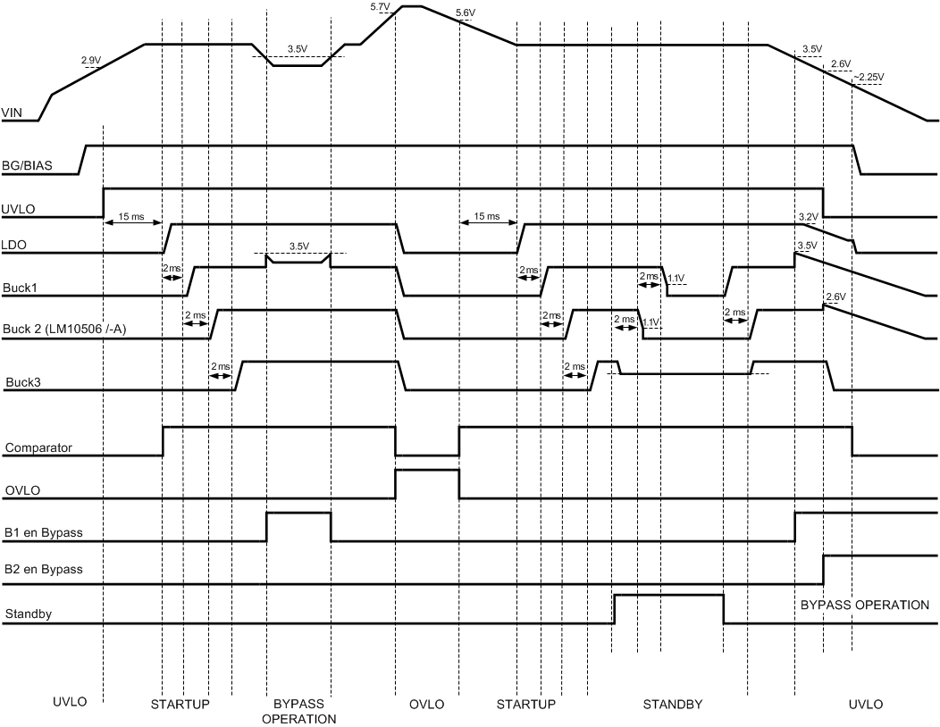 Figure 21. Operating Modes
8.3.2 Power-On Default And Device Enable
The device is always enabled and the LDO is always on, unless outside of operating voltage range. There is no LM10506 ENABLE Pin. Once VIN reaches a minimum required input Voltage the power-up sequence will be started automatically and the startup sequence will be initiated. Once the device is started, the output voltage of the Bucks 1 and 2 can be individually disabled by accessing their corresponding BKEN register bits (BUCK CONTROL).
8.3.3 RESET Pin Function
The RESET pin is internally pulled high. If the reset pin is pulled low, the device will perform a complete reset of all the registers to their default states. This means that all of the voltage settings on the regulators will go back to their default states.
8.3.4 Standby Function
The Device can be programmed into Standby mode. There are 2 ways for doing that:
- STANDBY pin
- Programming via SPI
8.3.4.1 STANDBY Pin
When the STANDBY pin is asserted high, the LM10506 will enter Standby Mode. While in Standby Mode, Buck 1 and Buck 2 are disabled. Buck 3’s output voltage is transitioned to the PSML (Programmable Standby Mode Level) as set by register 0x09. The STANDBY pin is internally pulled down, and there is a 1 second delay during powerup before the state of the STANDBY pin is checked.
NOTE
If Buck 1 and Buck 2 are already disabled, and the STANDBY pin is asserted high, then Buck 3 will not go to PSML – for further instructions, see STANDBY Programming via SPI.
Bucks 1 and 2 will be ramped down when the disable signal is given. Buck 1 starts ramping 2 ms after Buck 2 has started ramping.
Entering Standby Sequence will be:
- Buck 3 → PSML (Programmable Standby Mode Level)
- 2 ms delay
- Buck 2 → Disabled
- 2 ms delay
- Buck 1 → Disabled
An internal pulldown resistor 22 kΩ (±30%) is attached to the FB pin of Buck 1 and Buck 2. The outputs of Buck 1 and 2 are pulled to ground level when they are disabled to discharge any residual charge present in the output circuitry. When STANDBY transitions to a low, Buck 1 is again enabled followed by Buck 2. Buck 3 will go back to its previous state.
When waking up from Standby, the sequence will be:
- Buck 1 → Previous State
- 2 ms delay
- Buck 2 and Buck 3 transition together → Previous State
8.3.4.2 Standby Programming Via SPI
There is no bit which has the same function as the STANDBY pin. There is only one requirement programming LM10506 into Standby Mode via SPI. Setting LDO Sleep Mode bit high must be the last move when entering Standby Mode and programming the bit low when waking from Standby Mode must be the first move. Disabling or programming the Bucks to new level is the user’s decision based on power consumption and other requirements.
The following section describes how to program the chip into Standby Mode corresponding to STANDBY PIN function.
To program the LM10506 to Standby Mode via SPI Buck 1 and Buck 2 must be disabled by host device (Register 0x0A bit 1 and 0). Buck 3 must be programmed to desired level using Register 0x00. After Buck 3 has finished ramping LDO Sleep Mode bit must be set high (Register 0x0E bit 1). To wake LM10506 from Standby Mode LDO Sleep Mode bit must be set low (Register 0x0E bit 1). Bucks 1 and 2 must be enabled. Buck 3 voltage must be programmed to previous output level. For LM10506 -C, -D,when Buck 1 is re-enabled upon exiting STANDBY, soft start will engage.
8.3.4.3 Standby Mode, Operational Constraints
In Standby mode the device is in a low power mode. All internal clocks are turned off to conserve power and Buck 3 will only operate in PFM mode. While limited to PFM mode the loading on Buck 3 should be kept below 80 mA typ. to remain below the PFM/PWM threshold and avoid device shutdown. It is recommended that the device loading should be lowered accordingly prior to entering standby mode via STANDBY.
8.3.5 HL_B2, HL_B3 Function
The HL_B2/3 pins are digital pins which control alternate voltage selections of Buck 2 and Buck 3, respectively. HL_B2 has an internal pulldown which defaults to a 1.8-V output voltage selection for Buck 2. Alternatively, if HL_B2 is driven high, an output voltage of 3 V (or 2 V for LM10506-A) is selected. HL_B3 has an internal pull-up which defaults to a 1.2-V output voltage selection for Buck 3. Alternatively, if HL_B3 is driven low, an output voltage of 1 V is selected. The pull-up resistor is connected to the main input voltage. Transitions of the pins will not affect the output voltage, the state is only checked during start-up.
8.3.6 Undervoltage Lockout (UVLO)
The VIN voltage is monitored for a supply under voltage condition, for which the operation of the device can not be ensured. The part will automatically disable Buck 3. To prevent unstable operation, the undervoltage lockout (UVLO) has a hysteresis window of about 300 mV. An UVLO will force the device into the reset state, all internal registers are reset. Once the supply voltage is above the UVLO hysteresis, the device will initiate a power-up sequence and then enter the active state.
Buck 1 and Buck 2 will remain in bypass mode after VIN passes the UVLO until VIN reaches approximately 1.9 V. When Buck 2 is set to 1.8 V, the voltage will jump from 1.8 V to VUVLO_FALLING, and then follow VIN.
For LM10506 -C, -D,when Buck 1 is re-enabled upon exiting STANDBY, soft start will engage.
The LDO and the Comparator will remain functional past the UVLO threshold until VIN reaches approximately 2.25 V.
8.3.7 Overvoltage Lockout (OVLO)
The VIN voltage is monitored for a supply over voltage condition, for which the operation of the device cannot be ensured. The purpose of overvoltage lockout (OVLO) is to protect the part and all other consumers connected to the PMU outputs from any damage and malfunction. Once VIN rises over 5.7 V all the Bucks, and LDO will be disabled automatically. To prevent unstable operation, the OVLO has a hysteresis window of about 100 mV. An OVLO will force the device into the reset state; all internal registers are reset. Once the supply voltage is below the OVLO hysteresis, the device will initiate a power-up sequence, and then enter the active state. Operating maximum input voltage at which parameters are ensured is 5.5 V. Absolute maximum of the device is 6 V.
8.3.8 Interrupt Enable/Interrupt Status
The LM10506 has 2 interrupt registers, INTERRUPT ENABLE and INTERRUPT STATUS. These registers can be read via the serial interface. The interrupts are not latched to the register and will always represent the current state and will not be cleared on a read.
If interrupt condition is detected, then corresponding bit in the INTERRUPT STATUS register (0x0D) is set to '1', and IRQ output is asserted. There are 5 interrupt generating conditions:
- Buck 3 output is over flag level (90% when rising, 85% when falling)
- Buck 2 output is over flag level (90% when rising, 85% when falling)
- Buck 1 output is over flag level (90% when rising, 85% when falling)
- LDO is over flag level (90% when rising, 85% when falling
- Comparator input voltage crosses over selected threshold
Reading the interrupt register will not release IRQ output. Interrupt generation conditions can be individually enabled or disabled by writing respective bits in INTERRUPT ENABLE register (0x0C) to '1' or '0'.
8.3.9 Thermal Shutdown (TSD)
The temperature of the silicon die is monitored for an over-temperature condition, for which the operation of the device can not be ensured. The part will automatically be disabled if the temperature is too high. The thermal shutdown (TSD) will force the device into the reset state. In reset, all circuitry is disabled. To prevent unstable operation, the TSD has a hysteresis window of about 20°C. Once the temperature has decreased below the TSD hysteresis, the device will initiate a powerup sequence and then enter the active state. In the active state, the part will start up as if for the first time, all registers will be in their default state.
8.3.10 Comparator
The comparator on the LM10506 takes its inputs from the VCOMP pin and an internal threshold level which is programmed by the user. The threshold level is programmable between 2 V and 4 V with a step of 31 mV and a default comp code of 0x19. The output of the comparator is the IRQ pin. Its polarity can be changed using Register 0x0E bit 0. If IRQ_polarity = 0 → Active low (default) is selected, then the output is low if VCOMP value is greater than the threshold level. The output is high if the VCOMP value is less than the threshold level. If IRQ_polarity = 1 → Active high is selected then the output is high if VCOMP value is greater than the threshold level. The output is low if the VCOMP value is less than the threshold level. There is some hysteresis when VCOMP transitions from high to low, typically 60 mV. There is a control bit in register 0x0B, comparator control, that can double the hysteresis value.
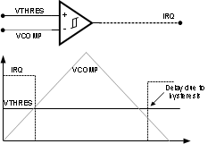 Figure 22.
8.4 Programming
8.4.1 SPI Data Interface
The device is programmable via 4-wire SPI Interface. The signals associated with this interface are CS, DI, DO and CLK. Through this interface, the user can enable/disable the device, program the output voltages of the individual bucks and of course read the status of Flag registers.
By accessing the registers in the device through this interface, the user can get access and control the operation of the buck controllers and program the reference voltage of the comparator in the device.
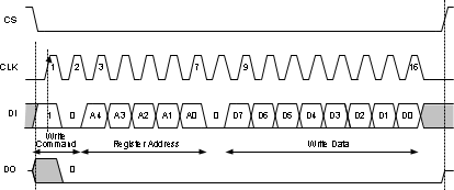 Figure 23. SPI Interface Write
- Data In (DI)
- 1 to 0 Write Command
- A4to A0 Register address to be written
- D7 to D0 Data to be written
- Data Out (DO)
- All Os
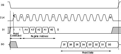 Figure 24. SPI Interface Read
- Data In (DI)
- 1 to 1 Read Command
- A4to A0 Register address to be read
- Data Out (DO)
- D7 to D0 Data Read
8.4.1.1 Registers Configurable via the SPI Interface
| ADDR | REG NAME | BIT | R/W | DEFAULT | DESCRIPTION | NOTES |
|---|---|---|---|---|---|---|
| 0x00 | Buck 3 Voltage | 7 | — | See Notes | Reset default: | |
| 6 | R/W | Buck 3 Voltage Code[6] | HL_B3 = 1 → 0x64 (1.2 V) | |||
| 5 | R/W | Buck 3 Voltage Code[5] | HL_B3 = 0 → 0x3C (1 V) | |||
| 4 | R/W | Buck 3 Voltage Code[4] | ||||
| 3 | R/W | Buck 3 Voltage Code[3] | Range: 0.7 V to 1.335 V | |||
| 2 | R/W | Buck 3 Voltage Code[2] | ||||
| 1 | R/W | Buck 3 Voltage Code[1] | ||||
| 0 | R/W | Buck 3 Voltage Code[0] | ||||
| 0x07 | Buck 1 Voltage | 7 | — | See Notes | Reset default: | |
| 6 | — | 0x26 (3 V) | ||||
| 5 | R/W | Buck 1 Voltage Code[5] | ||||
| 4 | R/W | Buck 1 Voltage Code[4] | Range: 1.1 V to 3.6 V | |||
| 3 | R/W | Buck 1 Voltage Code[3] | ||||
| 2 | R/W | Buck 1 Voltage Code[2] | ||||
| 1 | R/W | Buck 1 Voltage Code[1] | ||||
| 0 | R/W | Buck 1 Voltage Code[0] | ||||
| 0x08 | Buck 2 Voltage | 7 | — | See Notes | Reset default: | |
| 6 | — | HL_B2 = 1 → 0x26 (3 V)/ 0x12 (2 V for LM10506−A) |
||||
| 5 | R/W | Buck 2 Voltage Code[5] | HL_B2 = 0 → 0x0E (1.8 V) | |||
| 4 | R/W | Buck 2 Voltage Code[4] | ||||
| 3 | R/W | Buck 2 Voltage Code[3] | Range: 1.1 V to 3.6 V | |||
| 2 | R/W | Buck 2 Voltage Code[2] | ||||
| 1 | R/W | Buck 2 Voltage Code[1] | ||||
| 0 | R/W | Buck 2 Voltage Code[0] | ||||
| 0x09 | Standby Mode Voltage for Buck 3 |
7 | R/W | See Notes | Reset default: | |
| 6 | R/W | Buck 3 Voltage Code[6] | HL_B3 = 1 → 0x53 (1.115 V) | |||
| 5 | R/W | Buck 3 Voltage Code[5] | HL_B3 = 0 → 0x2E (0.93 V) | |||
| 4 | R/W | Buck 3 Voltage Code[4] | ||||
| 3 | R/W | Buck 3 Voltage Code[3] | ||||
| 2 | R/W | Buck 3 Voltage Code[2] | ||||
| 1 | R/W | Buck 3 Voltage Code[1] | ||||
| 0 | R/W | Buck 3 Voltage Code[0] | ||||
| 0x0A | Buck Control | 7 | R | 1 | BK3EN | Reads Buck 3 enable status |
| 6 | — | |||||
| 5 | — | |||||
| 4 | R/W | 0 | BK1FPWM | Buck 1 forced PWM mode when high | ||
| 3 | R/W | 0 | BK2FPWM | Buck 2 forced PWM mode when high | ||
| 2 | R/W | 0 | BK3FPWM | Buck 3 forced PWM mode when high | ||
| 1 | R/W | 1 | BK1EN | Enables Buck 1 0-disabled, 1-enabled | ||
| 0 | R/W | 1 | BK2EN | Enables Buck 2 0-disabled, 1-enabled | ||
| 0x0B | Comparator Control | 7 | R/W | 0 | Comp_hyst[0] | Doubles Comparator hysteresis |
| 6 | R/W | 0 | Comp_thres[5] | Programmable range of 2 V to 4 V, step size = 31.75 mV | ||
| 5 | R/W | 1 | Comp_thres[4] | Comparator Threshold reset default: 0x19 | ||
| 4 | R/W | 1 | Comp_thres[3] | |||
| 3 | R/W | 0 | Comp_thres[2] | Comp_hyst = 1 → min 80 mV hysteresis | ||
| 2 | R/W | 0 | Comp_thres[1] | Comp_hyst = 0 → min 40 mV hysteresis | ||
| 1 | R/W | 1 | Comp_thres[0] | |||
| 0 | R/W | 1 | COMPEN | Comparator enable | ||
| 0x0C | Interrupt Enable | 7 | — | |||
| 6 | — | |||||
| 5 | — | |||||
| 4 | R/W | 0 | LDO OK | |||
| 3 | R/W | 0 | Buck 3 OK | |||
| 2 | R/W | 0 | Buck 2 OK | |||
| 1 | R/W | 0 | Buck 1 OK | |||
| 0 | R/W | 1 | Comparator | Interrupt comp event | ||
| 0x0D | Interrupt Status | 7 | — | |||
| 6 | — | |||||
| 5 | — | |||||
| 4 | R | LDO OK | LDO is greater than 90% of target | |||
| 3 | R | Buck 3 OK | Buck 3 is greater than 90% of target | |||
| 2 | R | Buck 2 OK | Buck 2 is greater than 90% of target | |||
| 1 | R | Buck 1 OK | Buck 1 is greater than 90% of target | |||
| 0 | R | Comparator | Comparator output is high | |||
| 0x0E | MISC Control | 7 | — | |||
| 6 | — | |||||
| 5 | — | |||||
| 4 | — | |||||
| 3 | — | |||||
| 2 | — | |||||
| 1 | R/W | 0 | LDO Sleep Mode | LDO goes into extra power save mode | ||
| 0 | R/W | 0 | IRQ Polarity | IRQ_polarity = 0→Active low IRQ IRQ_polarity = 1→Active high IRQ |
8.4.1.1.1 ADDR 0x07& 0x08: Buck 1 And Buck 2 Voltage Code And VOUT Level Mapping
| VOLTAGE CODE | VOLTAGE (V) | VOLTAGE CODE | VOLTAGE (V) |
|---|---|---|---|
| 0x00 | 1.10 | 0x20 | 2.70 |
| 0x01 | 1.15 | 0x21 | 2.75 |
| 0x02 | 1.20 | 0x22 | 2.80 |
| 0x03 | 1.25 | 0x23 | 2.85 |
| 0x04 | 1.30 | 0x24 | 2.90 |
| 0x05 | 1.35 | 0x25 | 2.95 |
| 0x06 | 1.40 | 0x26 | 3.00 |
| 0x07 | 1.45 | 0x27 | 3.05 |
| 0x08 | 1.50 | 0x28 | 3.10 |
| 0x09 | 1.55 | 0x29 | 3.15 |
| 0x0A | 1.60 | 0x2A | 3.20 |
| 0x0B | 1.65 | 0x2B | 3.25 |
| 0x0C | 1.70 | 0x2C | 3.30 |
| 0x0D | 1.75 | 0x2D | 3.35 |
| 0x0E | 1.80 | 0x2E | 3.40 |
| 0x0F | 1.85 | 0x2F | 3.45 |
| 0x10 | 1.90 | 0x30 | 3.50 |
| 0x11 | 1.95 | 0x31 | 3.55 |
| 0x12 | 2.00 | 0x32 | 3.60 |
| 0x13 | 2.05 | 0x33 | 3.60 |
| 0x14 | 2.10 | 0x34 | 3.60 |
| 0x15 | 2.15 | 0x35 | 3.60 |
| 0x16 | 2.20 | 0x36 | 3.60 |
| 0x17 | 2.25 | 0x37 | 3.60 |
| 0x18 | 2.30 | 0x38 | 3.60 |
| 0x19 | 2.35 | 0x39 | 3.60 |
| 0x1A | 2.40 | 0x3A | 3.60 |
| 0x1B | 2.45 | 0x3B | 3.60 |
| 0x1C | 2.50 | 0x3C | 3.60 |
| 0x1D | 2.55 | 0x3D | 3.60 |
| 0x1E | 2.60 | 0x3E | 3.60 |
| 0x1F | 2.65 | 0x3F | 3.60 |
8.4.1.1.2 ADDR 0x00 & 0x09: Buck 3 Voltage Code And VOUT Level Mapping
| VOLTAGE CODE | VOLTAGE (V) | VOLTAGE CODE (V) | VOLTAGE (V) | VOLTAGE CODE | VOLTAGE (V) | VOLTAGE CODE | VOLTAGE (V) |
|---|---|---|---|---|---|---|---|
| 0x00 | 0.700 | 0x20 | 0.860 | 0x40 | 1.020 | 0x60 | 1.180 |
| 0x01 | 0.705 | 0x21 | 0.865 | 0x41 | 1.025 | 0x61 | 1.185 |
| 0x02 | 0.710 | 0x22 | 0.870 | 0x42 | 1.030 | 0x62 | 1.190 |
| 0x03 | 0.715 | 0x23 | 0.875 | 0x43 | 1.035 | 0x63 | 1.195 |
| 0x04 | 0.720 | 0x24 | 0.880 | 0x44 | 1.040 | 0x64 | 1.200 |
| 0x05 | 0.725 | 0x25 | 0.885 | 0x45 | 1.045 | 0x65 | 1.205 |
| 0x06 | 0.730 | 0x26 | 0.890 | 0x46 | 1.050 | 0x66 | 1.210 |
| 0x07 | 0.735 | 0x27 | 0.895 | 0x47 | 1.055 | 0x67 | 1.215 |
| 0x08 | 0.740 | 0x28 | 0.900 | 0x48 | 1.060 | 0x68 | 1.220 |
| 0x09 | 0.745 | 0x29 | 0.905 | 0x49 | 1.065 | 0x69 | 1.225 |
| 0x0A | 0.750 | 0x2A | 0.910 | 0x4A | 1.070 | 0x6A | 1.230 |
| 0x0B | 0.755 | 0x2B | 0.915 | 0x4B | 1.075 | 0x6B | 1.235 |
| 0x0C | 0.760 | 0x2C | 0.920 | 0x4C | 1.080 | 0x6C | 1.240 |
| 0x0D | 0.765 | 0x2D | 0.925 | 0x4D | 1.085 | 0x6D | 1.245 |
| 0x0E | 0.770 | 0x2E | 0.930 | 0x4E | 1.090 | 0x6E | 1.250 |
| 0x0F | 0.775 | 0x2F | 0.935 | 0x4F | 1.095 | 0x6F | 1.255 |
| 0x10 | 0.780 | 0x30 | 0.940 | 0x50 | 1.100 | 0x70 | 1.260 |
| 0x11 | 0.785 | 0x31 | 0.945 | 0x51 | 1.105 | 0x71 | 1.265 |
| 0x12 | 0.790 | 0x32 | 0.950 | 0x52 | 1.110 | 0x72 | 1.270 |
| 0x13 | 0.795 | 0x33 | 0.955 | 0x53 | 1.115 | 0x73 | 1.275 |
| 0x14 | 0.800 | 0x34 | 0.960 | 0x54 | 1.120 | 0x74 | 1.280 |
| 0x15 | 0.805 | 0x35 | 0.965 | 0x55 | 1.125 | 0x75 | 1.285 |
| 0x16 | 0.810 | 0x36 | 0.970 | 0x56 | 1.130 | 0x76 | 1.290 |
| 0x17 | 0.815 | 0x37 | 0.975 | 0x57 | 1.135 | 0x77 | 1.295 |
| 0x18 | 0.820 | 0x38 | 0.980 | 0x58 | 1.140 | 0x78 | 1.300 |
| 0x19 | 0.825 | 0x39 | 0.985 | 0x59 | 1.145 | 0x79 | 1.305 |
| 0x1A | 0.830 | 0x3A | 0.990 | 0x5A | 1.150 | 0x7A | 1.310 |
| 0x1B | 0.835 | 0x3B | 0.995 | 0x5B | 1.155 | 0x7B | 1.315 |
| 0x1C | 0.840 | 0x3C | 1.000 | 0x5C | 1.160 | 0x7C | 1.320 |
| 0x1D | 0.845 | 0x3D | 1.005 | 0x5D | 1.165 | 0x7D | 1.325 |
| 0x1E | 0.850 | 0x3E | 1.010 | 0x5E | 1.170 | 0x7E | 1.330 |
| 0x1F | 0.855 | 0x3F | 1.015 | 0x5F | 1.175 | 0x7F | 1.335 |
8.4.1.1.3 ADDR0x0B: Comparator Threshold Mapping
| VOLTAGE CODE | VOLTAGE (V) | VOLTAGE CODE | VOLTAGE (V) |
|---|---|---|---|
| 0x00 | 2.000 | 0x20 | 3.016 |
| 0x01 | 2.032 | 0x21 | 3.048 |
| 0x02 | 2.064 | 0x22 | 3.080 |
| 0x03 | 2.095 | 0x23 | 3.111 |
| 0x04 | 2.127 | 0x24 | 3.143 |
| 0x05 | 2.159 | 0x25 | 3.175 |
| 0x06 | 2.191 | 0x26 | 3.207 |
| 0x07 | 2.222 | 0x27 | 3.238 |
| 0x08 | 2.254 | 0x28 | 3.270 |
| 0x09 | 2.286 | 0x29 | 3.302 |
| 0x0A | 2.318 | 0x2A | 3.334 |
| 0x0B | 2.349 | 0x2B | 3.365 |
| 0x0C | 2.381 | 0x2C | 3.397 |
| 0x0D | 2.413 | 0x2D | 3.429 |
| 0x0E | 2.445 | 0x2E | 3.461 |
| 0x0F | 2.476 | 0x2F | 3.492 |
| 0x10 | 2.508 | 0x30 | 3.524 |
| 0x11 | 2.540 | 0x31 | 3.556 |
| 0x12 | 2.572 | 0x32 | 3.588 |
| 0x13 | 2.603 | 0x33 | 3.619 |
| 0x14 | 2.635 | 0x34 | 3.651 |
| 0x15 | 2.667 | 0x35 | 3.683 |
| 0x16 | 2.699 | 0x36 | 3.715 |
| 0x17 | 2.730 | 0x37 | 3.746 |
| 0x18 | 2.762 | 0x38 | 3.778 |
| 0x19 | 2.794 | 0x39 | 3.810 |
| 0x1A | 2.826 | 0x3A | 3.842 |
| 0x1B | 2.857 | 0x3B | 3.873 |
| 0x1C | 2.889 | 0x3C | 3.905 |
| 0x1D | 2.921 | 0x3D | 3.937 |
| 0x1E | 2.953 | 0x3E | 3.969 |
| 0x1F | 2.984 | 0x3F | 4.000 |