SNVS729F September 2011 – August 2014 LM10506
PRODUCTION DATA.
- 1 Features
- 2 Applications
- 3 Description
- 4 Revision History
- 5 Device Comparison Table
- 6 Pin Configuration and Functions
-
7 Specifications
- 7.1 Absolute Maximum Ratings
- 7.2 Handling Ratings
- 7.3 Recommended Operating Conditions
- 7.4 Thermal Information
- 7.5 General Electrical Characteristics
- 7.6 Buck 1 Electrical Characteristics
- 7.7 Buck 2 Electrical Characteristics
- 7.8 Buck 3 Electrical Characteristics
- 7.9 LDO Electrical Characteristics
- 7.10 Comparators Electrical Characteristics
- 7.11 Typical Characteristics
-
8 Detailed Description
- 8.1 Functional Block Diagram
- 8.2 Feature Description
- 8.3 Device Functional Modes
- 8.4 Programming
-
9 Application and Implementation
- 9.1 Application Information
- 9.2 Typical Application
- 10Power Supply Recommendations
- 11Layout
- 12Device and Documentation Support
- 13Mechanical, Packaging, and Orderable Information
Package Options
Mechanical Data (Package|Pins)
- YFR|34
Thermal pad, mechanical data (Package|Pins)
Orderable Information
11 Layout
11.1 Layout Guidelines
11.1.1 PCB Layout Considerations
PC board layout is an important part of DC-DC converter design. Poor board layout can disrupt the performance of a DC-DC converter and surrounding circuitry by contributing to EMI, ground bounce, and resistive voltage loss in the traces. These can send erroneous signals to the DC-DC converter resulting in poor regulation or instability. Good layout can be implemented by following a few simple design rules.
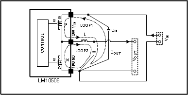 Schematic Of LM10506 Highlighting Layout Sensitive Nodes
- Minimize area of switched current loops. In a buck regulator there are two loops where currents are switched rapidly. The first loop starts from the CIN input capacitor, to the regulator SWx_VIN pin, to the regulator SW pin, to the inductor then out to the output capacitor COUT and load. The second loop starts from the output capacitor ground, to the regulator SWx_GND pins, to the inductor and then out to COUT and the load (see above). To minimize both loop areas the input capacitor should be placed as close as possible to the VIN pin. Grounding for both the input and output capacitors should consist of a small localized top side plane that connects to PGND. The inductor should be placed as close as possible to the SW pin and output capacitor.
- Minimize the copper area of the switch node. The SW pins should be directly connected with a trace that runs on top side directly to the inductor. To minimize IR losses this trace should be as short as possible and with a sufficient width. However, a trace that is wider than 100 mils will increase the copper area and cause too much capacitive loading on the SW pin. The inductors should be placed as close as possible to the SW pins to further minimize the copper area of the switch node.
- Have a single point ground for all device analog grounds. The ground connections for the feedback components should be connected together then routed to the GND pin of the device. This prevents any switched or load currents from flowing in the analog ground plane. If not properly handled, poor grounding can result in degraded load regulation or erratic switching behavior.
- Minimize trace length to the FB pin. The feedback trace should be routed away from the SW pin and inductor to avoid contaminating the feedback signal with switch noise.
- Make input and output bus connections as wide as possible. This reduces any voltage drops on the input or output of the converter and can improve efficiency. If voltage accuracy at the load is important make sure feedback voltage sense is made at the load. Doing so will correct for voltage drops at the load and provide the best output accuracy.
Outside 7x7 array 0.4 mm 34-bump DSBGA, with 24 peripheral and 6 inner vias = 30 individual signals
11.1.2 PCB Layout Thermal Dissipation For DSBGA Package
- Position ground layer as close as possible to DSBGA package. Second PCB layer is usually good option. LM10506 evaluation board is a good example.
- Draw power traces as wide as possible. Bumps which carry high currents should be connected to wide traces. This helps the silicon to cool down.
11.2 Layout Example
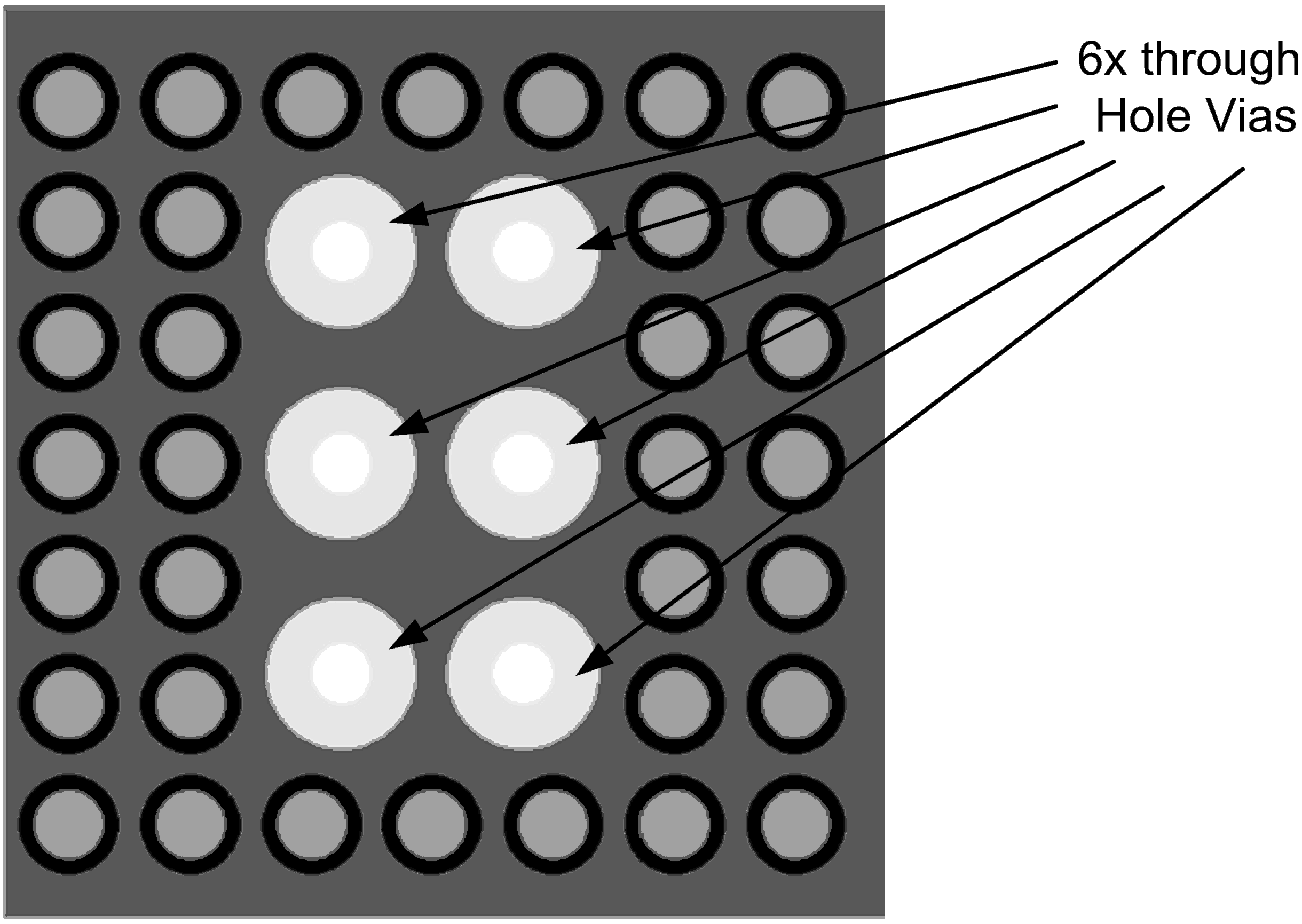 Figure 29. Possible PCB Layout Configuration
6x Through Hole Vias In The Middle