SNVS037H September 1999 – March 2024 LM1084
PRODUCTION DATA
- 1
- 1 Features
- 2 Applications
- 3 Description
- 4 Pin Configuration and Functions
- 5 Specifications
- 6 Detailed Description
-
7 Application and Implementation
- 7.1 Application Information
- 7.2
Typical Applications
- 7.2.1 1.2-V to 15-V Adjustable Regulator
- 7.2.2 Adjustable at 5 V
- 7.2.3 5-V Regulator With Shutdown
- 7.2.4 Battery Charger
- 7.2.5 Adjustable Fixed Regulator
- 7.2.6 Regulator with Reference
- 7.2.7 High Current Lamp Driver Protection
- 7.2.8 Battery Backup Regulated Supply
- 7.2.9 Ripple Rejection Enhancement
- 7.2.10 Automatic Light Control
- 7.2.11 Generating Negative Supply Voltage
- 7.2.12 Remote Sensing
- 7.3 Power Supply Recommendations
- 7.4 Layout
- 8 Device and Documentation Support
- 9 Revision History
- 10Mechanical, Packaging, and Orderable Information
Package Options
Mechanical Data (Package|Pins)
Thermal pad, mechanical data (Package|Pins)
- KTT|3
Orderable Information
4 Pin Configuration and Functions
 Figure 4-1 3-PinTO-220 PackageTop View
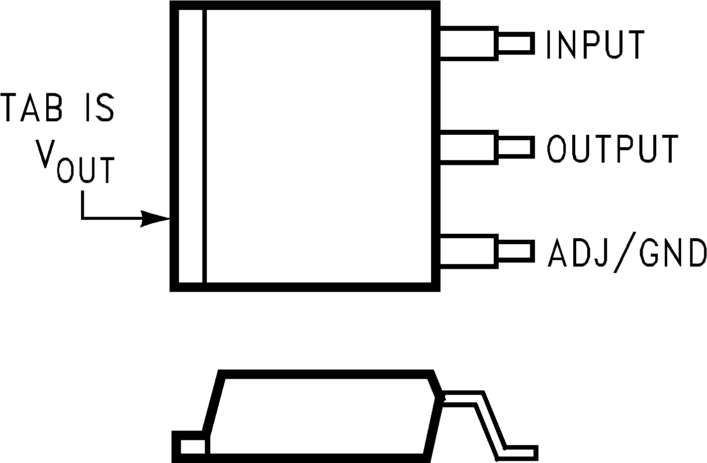
 Figure 4-2 3-PinTO-263 PackageTop View
Table 4-1 Pin Functions
| PIN | I/O | DESCRIPTION | |
|---|---|---|---|
| NAME | NO. | ||
| ADJ/GND | 1 | - | Adjust pin for the adjustable output voltage version. Ground pin for the fixed output voltage versions. |
| OUTPUT | 2 | O | Output voltage pin for the regulator. |
| INPUT | 3 | I | Input voltage pin for the regulator. |