SNVS039J June 2000 – April 2015 LM1086
PRODUCTION DATA.
- 1 Features
- 2 Applications
- 3 Description
- 4 Revision History
- 5 Pin Configuration and Functions
- 6 Specifications
- 7 Detailed Description
-
8 Application and Implementation
- 8.1 Application Information
- 8.2
Typical Applications
- 8.2.1 1.2-V to 15-V Adjustable Regulator
- 8.2.2 Adjustable at 5 V
- 8.2.3 5-V Regulator with Shutdown
- 8.2.4 Battery Charger
- 8.2.5 Adjustable Fixed Regulator
- 8.2.6 Regulator With Reference
- 8.2.7 High Current Lamp Driver Protection
- 8.2.8 Battery Backup Regulated Supply
- 8.2.9 Ripple Rejection Enhancement
- 8.2.10 Automatic Light Control
- 8.2.11 Remote Sensing
- 9 Power Supply Recommendations
- 10Layout
- 11Device and Documentation Support
- 12Mechanical, Packaging, and Orderable Information
Package Options
Mechanical Data (Package|Pins)
Thermal pad, mechanical data (Package|Pins)
- KTT|3
Orderable Information
7.1 Overview
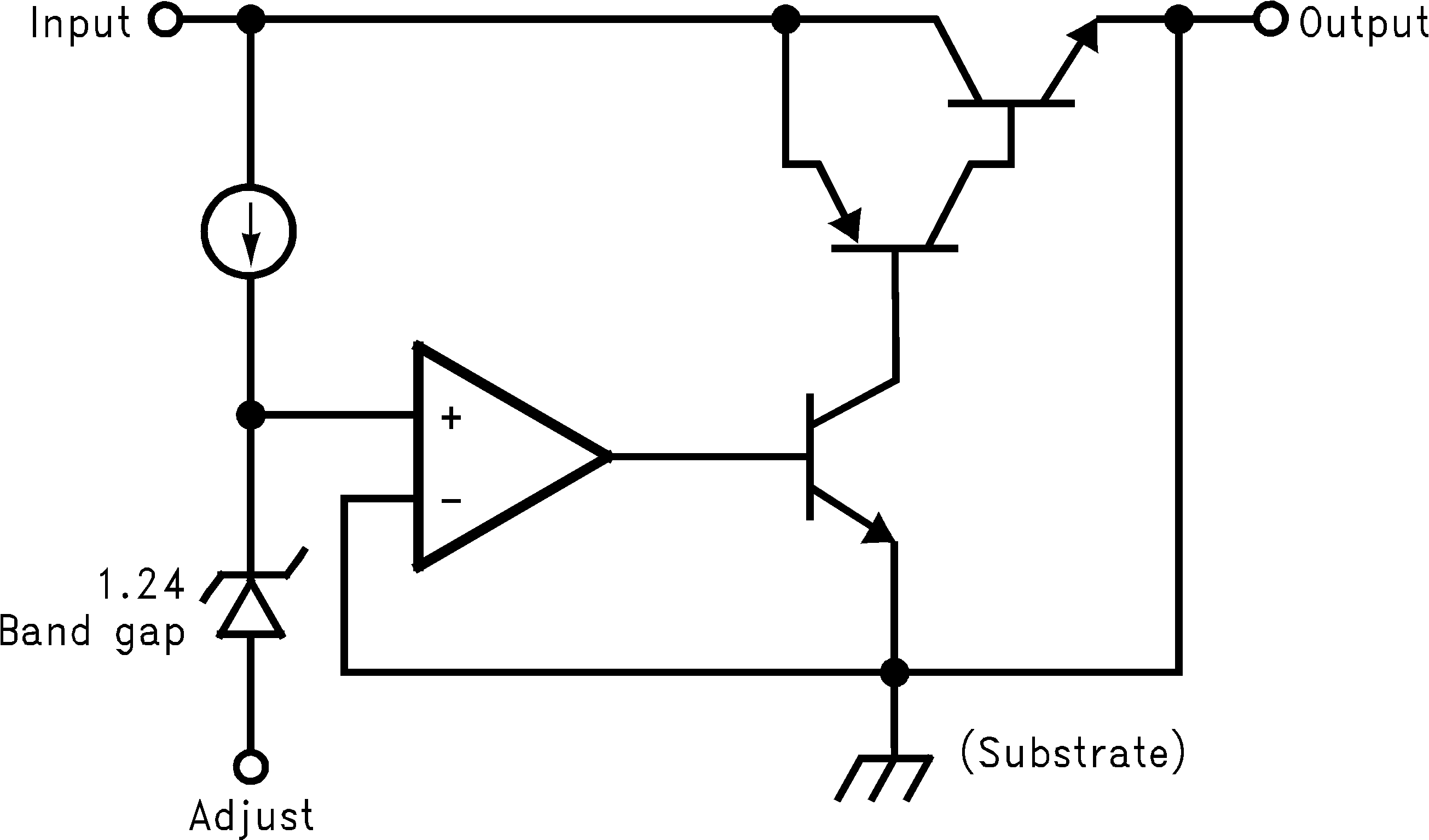
A basic functional diagram for the LM1086-ADJ (excluding protection circuitry) is shown in Figure 13. The topology is basically that of the LM317 except for the pass transistor. Instead of a Darlingtion NPN with its two diode voltage drop, the LM1086 uses a single NPN. This results in a lower dropout voltage. The structure of the pass transistor is also known as a quasi LDO. The advantage of a quasi LDO over a PNP LDO is its inherently lower quiescent current. The LM1086 is specified to provide a minimum dropout voltage of 1.5V over temperature, at full load.
 Figure 13. Basic Functional Block Diagram