SNVS039J June 2000 – April 2015 LM1086
PRODUCTION DATA.
- 1 Features
- 2 Applications
- 3 Description
- 4 Revision History
- 5 Pin Configuration and Functions
- 6 Specifications
- 7 Detailed Description
-
8 Application and Implementation
- 8.1 Application Information
- 8.2
Typical Applications
- 8.2.1 1.2-V to 15-V Adjustable Regulator
- 8.2.2 Adjustable at 5 V
- 8.2.3 5-V Regulator with Shutdown
- 8.2.4 Battery Charger
- 8.2.5 Adjustable Fixed Regulator
- 8.2.6 Regulator With Reference
- 8.2.7 High Current Lamp Driver Protection
- 8.2.8 Battery Backup Regulated Supply
- 8.2.9 Ripple Rejection Enhancement
- 8.2.10 Automatic Light Control
- 8.2.11 Remote Sensing
- 9 Power Supply Recommendations
- 10Layout
- 11Device and Documentation Support
- 12Mechanical, Packaging, and Orderable Information
Package Options
Mechanical Data (Package|Pins)
Thermal pad, mechanical data (Package|Pins)
- KTT|3
Orderable Information
8.2.6 Regulator With Reference
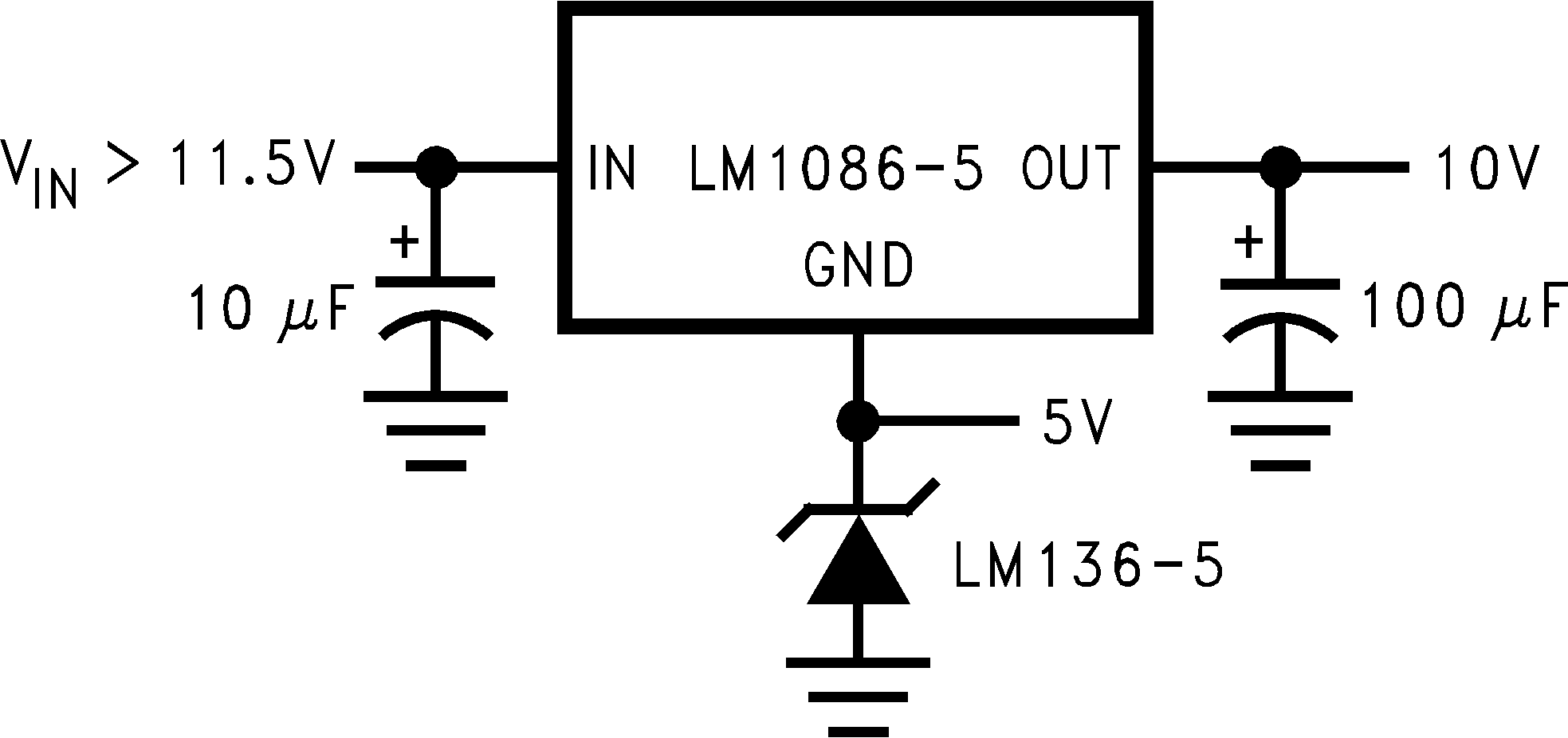
A fixed output voltage version of the LM1086-5.0 can be employed to provide an output rail and a reference rail at the same time as shown in Figure 23. This simple application makes use of a reference diode, the LM136-5, to regulate the GND voltage to a fixed 5 V based on the quiescent current generated by the GND pin. This voltage is then added onto the output to generate a total of 10 V out.
 Figure 23. Regulator With Reference