SNVS774Q May 2004 – June 2020 LM117 , LM317-N
PRODUCTION DATA.
- 1 Features
- 2 Applications
- 3 Description
- 4 Revision History
- 5 Device Comparison Table
- 6 Pin Configuration and Functions
- 7 Specifications
- 8 Detailed Description
-
9 Application and Implementation
- 9.1 Application Information
- 9.2
Typical Applications
- 9.2.1 1.25-V to 25-V Adjustable Regulator
- 9.2.2 5-V Logic Regulator With Electronic Shutdown
- 9.2.3 Slow Turnon 15-V Regulator
- 9.2.4 Adjustable Regulator With Improved Ripple Rejection
- 9.2.5 High Stability 10-V Regulator
- 9.2.6 High-Current Adjustable Regulator
- 9.2.7 Emitter-Follower Current Amplifier
- 9.2.8 1-A Current Regulator
- 9.2.9 Common-Emitter Amplifier
- 9.2.10 Low-Cost 3-A Switching Regulator
- 9.2.11 Current-Limited Voltage Regulator
- 9.2.12 Adjusting Multiple On-Card Regulators With Single Control
- 9.2.13 AC Voltage Regulator
- 9.2.14 12-V Battery Charger
- 9.2.15 Adjustable 4-A Regulator
- 9.2.16 Current-Limited 6-V Charger
- 9.2.17 Digitally Selected Outputs
- 10Power Supply Recommendations
- 11Layout
- 12Device and Documentation Support
- 13Mechanical, Packaging, and Orderable Information
Package Options
Mechanical Data (Package|Pins)
- NDS|2
Thermal pad, mechanical data (Package|Pins)
Orderable Information
11.1.1.1 Heatsink Requirements
The LM317-N regulators have internal thermal shutdown to protect the device from over-heating. Under all operating conditions, the junction temperature of the LM317-N must not exceed the rated maximum junction temperature (TJ) of 150°C for the LM117, or 125°C for the LM317-N. A heatsink may be required depending on the maximum device power dissipation and the maximum ambient temperature of the application. To determine if a heatsink is needed, the power dissipated by the regulator, PD, must be calculate with Equation 3:
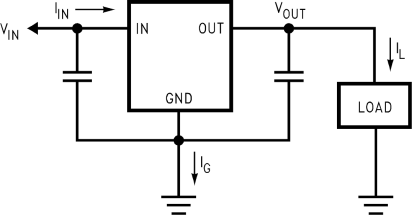
Figure 36 shows the voltage and currents which are present in the circuit.
The next parameter which must be calculated is the maximum allowable temperature rise, TR(MAX) in Equation 4:
where TJ(MAX) is the maximum allowable junction temperature (150°C for the LM117, or 125°C for the LM317-N), and TA(MAX) is the maximum ambient temperature that will be encountered in the application.
Using the calculated values for TR(MAX) and PD, the maximum allowable value for the junction-to-ambient thermal resistance (RθJA) can be calculated with Equation 5:
 Figure 36. Power Dissipation Diagram
 If the calculated maximum allowable thermal resistance is higher than the actual package rating, then no additional work is needed. If the calculated maximum allowable thermal resistance is lower than the actual package rating either the power dissipation (PD) needs to be reduced, the maximum ambient temperature TA(MAX) needs to be reduced, the thermal resistance (RθJA) must be lowered by adding a heatsink, or some combination of these.
If a heatsink is needed, the value can be calculated from Equation 6:
where
- θCH is the thermal resistance of the contact area between the device case and the heatsink surface
- RθJC is thermal resistance from the junction of the die to surface of the package case
When a value for θHA is found using the equation shown, a heatsink must be selected that has a value that is less than, or equal to, this number.
The θHA rating is specified numerically by the heatsink manufacturer in the catalog, or shown in a curve that plots temperature rise vs power dissipation for the heatsink.