SLCS160 June 2017 LM139-MIL
- 1 Features
- 2 Applications
- 3 Description
- 4 Revision History
- 5 Pin Configuration and Functions
- 6 Specifications
- 7 Detailed Description
- 8 Application and Implementation
- 9 Power Supply Recommendations
- 10Layout
- 11Device and Documentation Support
- 12Mechanical, Packaging, and Orderable Information
Package Options
Mechanical Data (Package|Pins)
Thermal pad, mechanical data (Package|Pins)
Orderable Information
5 Pin Configuration and Functions
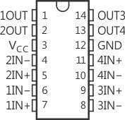
D, J, or W Package
SOIC, CDIP, or CFP
Top View

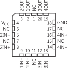
FK Package
20-Pin LCCC
Top View

NC = no internal connection.
Pin Functions
| PIN | I/O(1) | DESCRIPTION | ||
|---|---|---|---|---|
| NAME | D, J, W | FK | ||
| 1IN+ | 7 | 10 | I | Positive input pin of the comparator 1 |
| 1IN– | 6 | 9 | I | Negative input pin of the comparator 1 |
| 1OUT | 1 | 2 | O | Output pin of the comparator 1 |
| 2IN+ | 5 | 8 | I | Positive input pin of the comparator 2 |
| 2IN– | 4 | 6 | I | Negative input pin of the comparator 2 |
| 2OUT | 2 | 3 | O | Output pin of the comparator 2 |
| 3IN+ | 9 | 13 | I | Positive input pin of the comparator 3 |
| 3IN– | 8 | 12 | I | Negative input pin of the comparator 3 |
| 3OUT | 14 | 20 | O | Output pin of the comparator 3 |
| 4IN+ | 11 | 16 | I | Positive input pin of the comparator 4 |
| 4IN– | 10 | 14 | I | Negative input pin of the comparator 4 |
| 4OUT | 13 | 19 | O | Output pin of the comparator 4 |
| GND | 12 | 18 | — | Ground |
| VCC | 3 | 4 | — | Supply pin |
| NC | — | 1 | — | No connect (no internal connection) |
| 5 | ||||
| 7 | ||||
| 11 | ||||
| 15 | ||||
| 17 | ||||
(1) I = Input, O = Output