SNVS671F February 2011 – May 2019 LM21212-1
PRODUCTION DATA.
- 1 Features
- 2 Applications
- 3 Description
- 4 Revision History
- 5 Description
- 6 Pin Configuration and Functions
- 7 Specifications
- 8 Detailed Description
- 9 Application and Implementation
- 10Layout
- 11Device and Documentation Support
- 12Mechanical, Packaging, And Orderable Information
Package Options
Mechanical Data (Package|Pins)
- PWP|20
Thermal pad, mechanical data (Package|Pins)
- PWP|20
Orderable Information
10.1 Pcb Layout Considerations
PC board layout is an important part of DC-DC converter design. Poor board layout can disrupt the performance of a DC-DC converter and surrounding circuitry by contributing to EMI, ground bounce, and resistive voltage loss in the traces. These can send erroneous signals to the DC-DC converter resulting in poor regulation or instability.
Good layout can be implemented by following a few simple design rules.
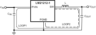
- Minimize area of switched current loops. In a buck regulator there are two loops where currents are switched at high slew rates. The first loop starts from the input capacitor, to the regulator PVIN pin, to the regulator SW pin, to the inductor then out to the output capacitor and load. The second loop starts from the output capacitor ground, to the regulator GND pins, to the inductor and then out to the load (see Figure 37). To minimize both loop areas, the input capacitor should be placed as close as possible to the VIN pin. Grounding for both the input and output capacitor should be close. Ideally, a ground plane should be placed on the top layer that connects the PGND pins, the exposed pad (EP) of the device, and the ground connections of the input and output capacitors in a small area near pin 10 and 11 of the device. The inductor should be placed as close as possible to the SW pin and output capacitor.
- Minimize the copper area of the switch node. The six SW pins should be routed on a single top plane to the pad of the inductor. The inductor should be placed as close as possible to the switch pins of the device with a wide trace to minimize conductive losses. The inductor can be placed on the bottom side of the PCB relative to the LM21212-1, but care must be taken to not allow any coupling of the magnetic field of the inductor into the sensitive feedback or compensation traces.
- Have a solid ground plane between PGND, the EP and the input and output cap. ground connections. The ground connections for the AGND, compensation, feedback, and soft-start components should be physically isolated (located near pin 1 and 20) from the power ground plane but a separate ground connection is not necessary. If not properly handled, poor grounding can result in degraded load regulation or erratic switching behavior.
- Carefully route the connection from the VOUT signal to the compensation network. This node is high impedance and can be susceptible to noise coupling. The trace should be routed away from the SW pin and inductor to avoid contaminating the feedback signal with switch noise.
- Make input and output bus connections as wide as possible. This reduces any voltage drops on the input or output of the converter and can improve efficiency. Voltage accuracy at the load is important so make sure feedback voltage sense is made at the load. Doing so will correct for voltage drops at the load and provide the best output accuracy.
- Provide adequate device heatsinking. For most 12A designs a four layer board is recommended. Use as many vias as is possible to connect the EP to the power plane heatsink. The vias located underneith the EP will wick solder into them if they are not filled. Complete solder coverage of the EP to the board is required to achieve the θJA values described in the previous section. Either an adequate amount of solder must be applied to the EP pad to fill the vias, or the vias must be filled during manufacturing. See the Thermal Considerations section to ensure enough copper heatsinking area is used to keep the junction temperature below 125°C.
 Figure 37. Schematic Of Lm21212-1 Highlighting Layout Sensitive Nodes
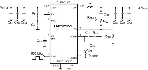
  Figure 38. Typical Application Schematic 1
 Table 1. Bill Of Materials (VIN = 3.3 - 5.5v, VOUT = 1.2v, IOUT = 12a, FSW = 500khz)
| ID | DESCRIPTION | VENDOR | PART NUMBER | QUANTITY |
|---|---|---|---|---|
| CF | CAP, CERM, 1uF, 10V, +/-10%, X7R, 0603 | MuRata | GRM188R71A105KA61D | 1 |
| CIN1, CIN2, CIN3, CO1, CO2, CO3 | CAP, CERM, 100uF, 6.3V, +/-20%, X5R, 1206 | MuRata | GRM31CR60J107ME39L | 6 |
| CC1 | CAP, CERM, 1800pF, 50V, +/-5%, C0G/NP0, 0603 | TDK | C1608C0G1H182J | 1 |
| CC2 | CAP, CERM, 68pF, 50V, +/-5%, C0G/NP0, 0603 | TDK | C1608C0G1H680J | 1 |
| CC3 | CAP, CERM, 820pF, 50V, +/-5%, C0G/NP0, 0603 | TDK | C1608C0G1H821J | 1 |
| CSS | CAP, CERM, 0.033uF, 16V, +/-10%, X7R, 0603 | MuRata | GRM188R71C333KA01D | 1 |
| LO | Inductor, Shielded Drum Core, Powdered Iron, 560nH, 27.5A, 0.0018 ohm, SMD | Vishay-Dale | IHLP4040DZERR56M01 | 1 |
| RF | RES, 1.0 ohm, 5%, 0.1W, 0603 | Vishay-Dale | CRCW06031R00JNEA | 1 |
| RC1 | RES, 9.31k ohm, 1%, 0.1W, 0603 | Vishay-Dale | CRCW06039K31FKEA | 1 |
| RC2 | RES, 165 ohm, 1%, 0.1W, 0603 | Vishay-Dale | CRCW0603165RFKEA | 1 |
| RFB1, RFB2, RPGOOD | RES, 10k ohm, 1%, 0.1W, 0603 | Vishay-Dale | CRCW060310K0FKEA | 3 |
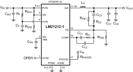
 Figure 39. Typical Application Schematic 2