SNVS625G February   2011  – March 2022 LM21215

PRODUCTION DATA  

  1. Features
  2. Applications
  3. Description
  4. Revision History
  5. Pin Configuration and Functions
  6. Specifications
    1. 6.1 Absolute Maximum Ratings
    2. 6.2 ESD Ratings
    3. 6.3 Recommended Operating Ratings
    4. 6.4 Electrical Characteristics
    5. 6.5 Typical Characteristics
  7. Detailed Description
    1. 7.1 Overview
    2. 7.2 Functional Block Diagram
    3. 7.3 Feature Description
      1. 7.3.1 Precision Enable
      2. 7.3.2 UVLO
      3. 7.3.3 Current Limit
      4. 7.3.4 Short-Circuit Protection
      5. 7.3.5 Thermal Protection
      6. 7.3.6 Light Load Operation
      7. 7.3.7 Power Good Flag
    4. 7.4 Device Functional Modes
  8. Application and Implementation
    1. 8.1 Application Information
    2. 8.2 Typical Application
      1. 8.2.1 Typical Application 1
        1. 8.2.1.1 Design Requirements
        2. 8.2.1.2 Detailed Design Procedure
          1. 8.2.1.2.1 Custom Design With WEBENCH® Tools
          2. 8.2.1.2.2 Output Voltage
          3. 8.2.1.2.3 Precision Enable
          4. 8.2.1.2.4 Soft Start
          5. 8.2.1.2.5 Inductor Selection
          6. 8.2.1.2.6 Output Capacitor Selection
          7. 8.2.1.2.7 Input Capacitor Selection
          8. 8.2.1.2.8 Programmable Current Limit
          9. 8.2.1.2.9 Control Loop Compensation
        3. 8.2.1.3 Application Curves
      2. 8.2.2 Typical Application Schematic 2
        1. 8.2.2.1 Design Requirements
        2. 8.2.2.2 Detailed Design Procedure
  9. Layout
    1. 9.1 Layout Considerations
    2. 9.2 Layout Example
      1. 9.2.1 Thermal Considerations
  10. 10Device and Documentation Support
    1. 10.1 Device Support
      1. 10.1.1 Third-Party Products Disclaimer
      2. 10.1.2 Development Support
        1. 10.1.2.1 Custom Design With WEBENCH® Tools
    2. 10.2 Receiving Notification of Documentation Updates
    3. 10.3 Support Resources
    4. 10.4 Trademarks
    5. 10.5 Electrostatic Discharge Caution
    6. 10.6 Glossary
  11. 11Mechanical, Packaging, and Orderable Information

Package Options

Mechanical Data (Package|Pins)
Thermal pad, mechanical data (Package|Pins)
Orderable Information
Precision Enable

The enable (EN) pin of the LM21215 allows the output to be toggled on and off. This pin is a precision analog input. When the voltage exceeds 1.35 V, the controller will try to regulate the output voltage as long as the input voltage has exceeded the UVLO voltage of 2.7 V. There is an internal current source connected to EN so if enable is not used, the device will turn on automatically. If EN is not toggled directly, the device can be pre-programmed to turn on at a certain input voltage higher than the UVLO voltage. This can be done with an external resistor divider from AVIN to EN and EN to AGND as shown in Figure 8-3.
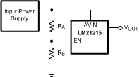
GUID-8EE651EF-2A21-40E6-AE56-5F4F0F88B4D4-low.gifFigure 8-3 Enable Start-Up Through VIN

The resistor values of RA and RB can be relatively sized to allow EN to reach the enable threshold voltage depending on the input supply voltage. With the enable current source accounted for, the equation solving for RA is the following:

Equation 3. GUID-6AD525F7-025D-4815-BF50-3A176367FEEC-low.gif

where

  • RA is the resistor from VIN to enable.
  • RB is the resistor from enable to ground.
  • IEN is the internal enable pullup current (2 µA).
  • 1.35 V is the fixed precision enable threshold voltage.

Typical values for RB range from 10 kΩ to 100 kΩ.