SNVS625G February   2011  – March 2022 LM21215

PRODUCTION DATA  

  1. Features
  2. Applications
  3. Description
  4. Revision History
  5. Pin Configuration and Functions
  6. Specifications
    1. 6.1 Absolute Maximum Ratings
    2. 6.2 ESD Ratings
    3. 6.3 Recommended Operating Ratings
    4. 6.4 Electrical Characteristics
    5. 6.5 Typical Characteristics
  7. Detailed Description
    1. 7.1 Overview
    2. 7.2 Functional Block Diagram
    3. 7.3 Feature Description
      1. 7.3.1 Precision Enable
      2. 7.3.2 UVLO
      3. 7.3.3 Current Limit
      4. 7.3.4 Short-Circuit Protection
      5. 7.3.5 Thermal Protection
      6. 7.3.6 Light Load Operation
      7. 7.3.7 Power Good Flag
    4. 7.4 Device Functional Modes
  8. Application and Implementation
    1. 8.1 Application Information
    2. 8.2 Typical Application
      1. 8.2.1 Typical Application 1
        1. 8.2.1.1 Design Requirements
        2. 8.2.1.2 Detailed Design Procedure
          1. 8.2.1.2.1 Custom Design With WEBENCH® Tools
          2. 8.2.1.2.2 Output Voltage
          3. 8.2.1.2.3 Precision Enable
          4. 8.2.1.2.4 Soft Start
          5. 8.2.1.2.5 Inductor Selection
          6. 8.2.1.2.6 Output Capacitor Selection
          7. 8.2.1.2.7 Input Capacitor Selection
          8. 8.2.1.2.8 Programmable Current Limit
          9. 8.2.1.2.9 Control Loop Compensation
        3. 8.2.1.3 Application Curves
      2. 8.2.2 Typical Application Schematic 2
        1. 8.2.2.1 Design Requirements
        2. 8.2.2.2 Detailed Design Procedure
  9. Layout
    1. 9.1 Layout Considerations
    2. 9.2 Layout Example
      1. 9.2.1 Thermal Considerations
  10. 10Device and Documentation Support
    1. 10.1 Device Support
      1. 10.1.1 Third-Party Products Disclaimer
      2. 10.1.2 Development Support
        1. 10.1.2.1 Custom Design With WEBENCH® Tools
    2. 10.2 Receiving Notification of Documentation Updates
    3. 10.3 Support Resources
    4. 10.4 Trademarks
    5. 10.5 Electrostatic Discharge Caution
    6. 10.6 Glossary
  11. 11Mechanical, Packaging, and Orderable Information

Package Options

Mechanical Data (Package|Pins)
Thermal pad, mechanical data (Package|Pins)
Orderable Information

Application Curves

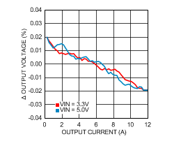
GUID-E3805F6F-6BD0-48B0-91DF-A35B0AAF5154-low.gifFigure 8-10 Load Regulation
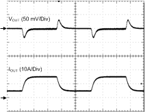
GUID-85DCB10E-431E-4847-9708-51FB069086DD-low.gif
                                            100 µs/DIV
Figure 8-12 Load Transient Response
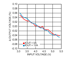
GUID-348D5CF4-A6B8-4E78-B522-705733EE965A-low.gifFigure 8-11 Line Regulation
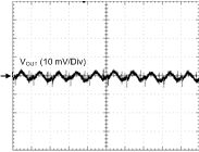
GUID-9BB47DE6-F21A-4707-9A1E-8AD660D312F8-low.gif
                                            2 µs/DIV
Figure 8-13 Output Voltage Ripple (IOUT = 15 A)