SNOSB87D March 2011 – May 2019 LM21215A
PRODUCTION DATA.
- 1 Features
- 2 Applications
- 3 Description
- 4 Revision History
- 5 Pin Configuration and Functions
- 6 Specifications
- 7 Detailed Description
- 8 Application and Implementation
- 9 Power Supply Recommendations
- 10Layout
- 11Device and Documentation Support
- 12Mechanical, Packaging, and Orderable Information
Package Options
Mechanical Data (Package|Pins)
- PWP|20
Thermal pad, mechanical data (Package|Pins)
- PWP|20
Orderable Information
8.2.1.2.4 Filter Inductor Selection
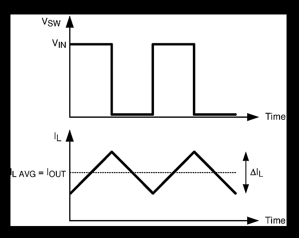
The filter inductor, designated LF, chosen for the application influences the ripple current and the efficiency of the converter. The first selection criteria is to define the buck converter inductor ripple current ΔIL, typically selected between 20% to 40% of the maximum output current. Figure 31 shows the ripple current in a conventional buck converter operating in continuous conduction mode. Larger ripple current results in a lower inductance, which leads to lower inductor DC resistance (DCR) and improved efficiency. However, larger ripple current causes the LM21215A to operate in DCM at a higher average output current.
 Figure 31. Switch (SW) Voltage and Inductor Current Waveforms
 Once the ripple current has been determined, calculate the appropriate inductance using Equation 5.

A 0.56-µH inductor with 1.8-mΩ DCR meets the application requirements here. The peak inductor current at full load corresponds to the maximum output current plus the ripple current, as shown by Equation 6.

Choose an inductor with a saturation current rating at maximum operating temperature that is higher than the overcurrent protection limit. In general, lower inductance is desirable in switching converters because it equates to faster transient response, lower inductor DCR, and reduced size for more compact designs. However, too low of an inductance implies large inductor ripple current such that the overcurrent protection circuit is falsely triggered at the full load. Larger inductor ripple current also implies higher output voltage ripple.