SNOSB87D March   2011  – May 2019 LM21215A

PRODUCTION DATA.  

  1. Features
  2. Applications
    1.     Efficiency at 2.5 V, 500 kHz
  3. Description
    1.     Typical Application Circuit
      1.      Device Images
  4. Revision History
  5. Pin Configuration and Functions
    1.     Pin Functions
  6. Specifications
    1. 6.1 Absolute Maximum Ratings
    2. 6.2 ESD Ratings
    3. 6.3 Recommended Operating Conditions
    4. 6.4 Thermal Information
    5. 6.5 Electrical Characteristics
    6. 6.6 Typical Characteristics
  7. Detailed Description
    1. 7.1 Overview
    2. 7.2 Functional Block Diagram
    3. 7.3 Feature Description
      1. 7.3.1 Precision Enable
      2. 7.3.2 Input Voltage UVLO
      3. 7.3.3 Soft-Start Capability
      4. 7.3.4 PGOOD Indicator
      5. 7.3.5 Frequency Synchronization
      6. 7.3.6 Current Limit
      7. 7.3.7 Short Circuit Protection
    4. 7.4 Device Functional Modes
      1. 7.4.1 Light-Load Operation
      2. 7.4.2 Overvoltage and Undervoltage Handling
      3. 7.4.3 Thermal Shutdown
  8. Application and Implementation
    1. 8.1 Application Information
    2. 8.2 Typical Applications
      1. 8.2.1 Typical Application 1
        1. 8.2.1.1 Design Requirements
        2. 8.2.1.2 Detailed Design Procedure
          1. 8.2.1.2.1 Custom Design With WEBENCH® Tools
          2. 8.2.1.2.2 Output Voltage Setpoint
          3. 8.2.1.2.3 Precision Enable
          4. 8.2.1.2.4 Filter Inductor Selection
          5. 8.2.1.2.5 Output Capacitor Selection
          6. 8.2.1.2.6 Input Capacitor Selection
          7. 8.2.1.2.7 Control Loop Compensation
        3. 8.2.1.3 Application Curves
      2. 8.2.2 Typical Application 2
        1. 8.2.2.1 Design Requirements
        2. 8.2.2.2 Detailed Design Procedure
  9. Power Supply Recommendations
  10. 10Layout
    1. 10.1 Layout Guidelines
      1. 10.1.1 Compact PCB Layout for EMI Reduction
      2. 10.1.2 Thermal Design
      3. 10.1.3 Ground Plane Design
    2. 10.2 Layout Example
  11. 11Device and Documentation Support
    1. 11.1 Device Support
      1. 11.1.1 Third-Party Products Disclaimer
      2. 11.1.2 Development Support
        1. 11.1.2.1 Custom Design With WEBENCH® Tools
    2. 11.2 Documentation Support
      1. 11.2.1 Related Documentation
    3. 11.3 Community Resources
    4. 11.4 Trademarks
    5. 11.5 Electrostatic Discharge Caution
    6. 11.6 Glossary
  12. 12Mechanical, Packaging, and Orderable Information

Package Options

Mechanical Data (Package|Pins)
Thermal pad, mechanical data (Package|Pins)
Orderable Information

Output Voltage Setpoint

The first step in designing an LM21215A application is to configure the output voltage setpoint by using a voltage divider between VOUT and AGND, with the middle node connected to FB. When operating under steady state conditions, the LM21215A regulates VOUT such that the FB voltage is driven to 0.6 V.
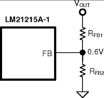
LM21215A FB_divider_nosb87.gifFigure 29. Setting the Output Voltage by Feedback Resistor Divider

A good starting point for the lower feedback resistor, RFB2, is 10 kΩ. Calculate RFB1 using Equation 3.

Equation 3. LM21215A q_Vout_nosb87.gif