SNOSB87D March   2011  – May 2019 LM21215A

PRODUCTION DATA.  

  1. Features
  2. Applications
    1.     Efficiency at 2.5 V, 500 kHz
  3. Description
    1.     Typical Application Circuit
      1.      Device Images
  4. Revision History
  5. Pin Configuration and Functions
    1.     Pin Functions
  6. Specifications
    1. 6.1 Absolute Maximum Ratings
    2. 6.2 ESD Ratings
    3. 6.3 Recommended Operating Conditions
    4. 6.4 Thermal Information
    5. 6.5 Electrical Characteristics
    6. 6.6 Typical Characteristics
  7. Detailed Description
    1. 7.1 Overview
    2. 7.2 Functional Block Diagram
    3. 7.3 Feature Description
      1. 7.3.1 Precision Enable
      2. 7.3.2 Input Voltage UVLO
      3. 7.3.3 Soft-Start Capability
      4. 7.3.4 PGOOD Indicator
      5. 7.3.5 Frequency Synchronization
      6. 7.3.6 Current Limit
      7. 7.3.7 Short Circuit Protection
    4. 7.4 Device Functional Modes
      1. 7.4.1 Light-Load Operation
      2. 7.4.2 Overvoltage and Undervoltage Handling
      3. 7.4.3 Thermal Shutdown
  8. Application and Implementation
    1. 8.1 Application Information
    2. 8.2 Typical Applications
      1. 8.2.1 Typical Application 1
        1. 8.2.1.1 Design Requirements
        2. 8.2.1.2 Detailed Design Procedure
          1. 8.2.1.2.1 Custom Design With WEBENCH® Tools
          2. 8.2.1.2.2 Output Voltage Setpoint
          3. 8.2.1.2.3 Precision Enable
          4. 8.2.1.2.4 Filter Inductor Selection
          5. 8.2.1.2.5 Output Capacitor Selection
          6. 8.2.1.2.6 Input Capacitor Selection
          7. 8.2.1.2.7 Control Loop Compensation
        3. 8.2.1.3 Application Curves
      2. 8.2.2 Typical Application 2
        1. 8.2.2.1 Design Requirements
        2. 8.2.2.2 Detailed Design Procedure
  9. Power Supply Recommendations
  10. 10Layout
    1. 10.1 Layout Guidelines
      1. 10.1.1 Compact PCB Layout for EMI Reduction
      2. 10.1.2 Thermal Design
      3. 10.1.3 Ground Plane Design
    2. 10.2 Layout Example
  11. 11Device and Documentation Support
    1. 11.1 Device Support
      1. 11.1.1 Third-Party Products Disclaimer
      2. 11.1.2 Development Support
        1. 11.1.2.1 Custom Design With WEBENCH® Tools
    2. 11.2 Documentation Support
      1. 11.2.1 Related Documentation
    3. 11.3 Community Resources
    4. 11.4 Trademarks
    5. 11.5 Electrostatic Discharge Caution
    6. 11.6 Glossary
  12. 12Mechanical, Packaging, and Orderable Information

Package Options

Mechanical Data (Package|Pins)
Thermal pad, mechanical data (Package|Pins)
Orderable Information

PGOOD Indicator

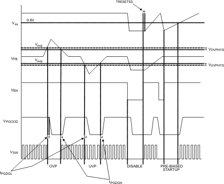
The PGOOD flag provides the user with a way to monitor the status of the LM21215A. In order to use the PGOOD function, the application must provide a pullup resistor to a desired DC voltage, for example VIN. PGOOD responds to a fault condition by pulling PGOOD low with the open-drain output. PGOOD pulls low on the following conditions: 1) VFB moves above or below the VOVP or VUVP, respectively; 2) The EN voltage is brought below the Enable turn-off threshold; 3) A pre-biased output condition exists (VFB > VSS/TRK). PGOOD has 12 μs and 15 μs of built-in deglitch time for rising and falling edges, respectively.

Figure 24 shows the conditions that cause PGOOD to respond.
LM21215A 30152118_nosb87.gifFigure 24. PGOOD Indicator Operation