SNOSB87D March 2011 – May 2019 LM21215A
PRODUCTION DATA.
- 1 Features
- 2 Applications
- 3 Description
- 4 Revision History
- 5 Pin Configuration and Functions
- 6 Specifications
- 7 Detailed Description
- 8 Application and Implementation
- 9 Power Supply Recommendations
- 10Layout
- 11Device and Documentation Support
- 12Mechanical, Packaging, and Orderable Information
Package Options
Mechanical Data (Package|Pins)
- PWP|20
Thermal pad, mechanical data (Package|Pins)
- PWP|20
Orderable Information
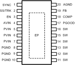
5 Pin Configuration and Functions
PWP Package
20-Pin HTSSOP With Exposed Thermal Pad
Top View

Pin Functions
| PIN | TYPE(1) | DESCRIPTION | |
|---|---|---|---|
| NO. | NAME | ||
| 1 | SYNC | I | Frequency synchronization input pin. Applying a clock signal to this pin forces the device to switch at the clock frequency. If left unconnected, the frequency defaults to 500 kHz. |
| 2 | SS/TRK | I | Soft-start control pin. An internal 2-µA current source charges an external capacitor connected between this pin and AGND to set the output voltage ramp rate during startup. This pin can also be used to configure the tracking feature. |
| 3 | EN | I | Active high precision enable input. If not used, the EN pin can be left open, which will go high due to an internal pullup current source. |
| 4 | AVIN | P | Analog input voltage supply that generates the internal bias. Connect PVIN to AVIN through a low pass RC filter to minimize the influence of input rail ripple and noise on the analog control circuitry. |
| 5–7 | PVIN | P | Input voltage to the power switches inside the device. Connect these pins together at the device. Locate a low ESR input capacitance as close as possible to these pins. |
| 8–10 | PGND | G | Power ground pins for the internal power switches. |
| 11–16 | SW | P | Switch node pins. Tie these pins together locally and connect to the filter inductor. |
| 17 | PGOOD | O | Open-drain power good indicator. |
| 18 | COMP | O | Compensation pin is connected to the output of the voltage loop error amplifier. |
| 19 | FB | I | Feedback pin is connected to the inverting input of the voltage loop error amplifier. |
| 20 | AGND | G | Quiet analog ground for the internal reference and bias circuitry. |
| EP | Exposed Pad | P | Exposed metal pad on the underside of the package with an electrical and thermal connection to PGND. Connect this pad to the PC board ground plane to improve thermal dissipation. |
(1) P = Power, G = Ground, I = Input, O = Output.