SNOSB87D March   2011  – May 2019 LM21215A

PRODUCTION DATA.  

  1. Features
  2. Applications
    1.     Efficiency at 2.5 V, 500 kHz
  3. Description
    1.     Typical Application Circuit
      1.      Device Images
  4. Revision History
  5. Pin Configuration and Functions
    1.     Pin Functions
  6. Specifications
    1. 6.1 Absolute Maximum Ratings
    2. 6.2 ESD Ratings
    3. 6.3 Recommended Operating Conditions
    4. 6.4 Thermal Information
    5. 6.5 Electrical Characteristics
    6. 6.6 Typical Characteristics
  7. Detailed Description
    1. 7.1 Overview
    2. 7.2 Functional Block Diagram
    3. 7.3 Feature Description
      1. 7.3.1 Precision Enable
      2. 7.3.2 Input Voltage UVLO
      3. 7.3.3 Soft-Start Capability
      4. 7.3.4 PGOOD Indicator
      5. 7.3.5 Frequency Synchronization
      6. 7.3.6 Current Limit
      7. 7.3.7 Short Circuit Protection
    4. 7.4 Device Functional Modes
      1. 7.4.1 Light-Load Operation
      2. 7.4.2 Overvoltage and Undervoltage Handling
      3. 7.4.3 Thermal Shutdown
  8. Application and Implementation
    1. 8.1 Application Information
    2. 8.2 Typical Applications
      1. 8.2.1 Typical Application 1
        1. 8.2.1.1 Design Requirements
        2. 8.2.1.2 Detailed Design Procedure
          1. 8.2.1.2.1 Custom Design With WEBENCH® Tools
          2. 8.2.1.2.2 Output Voltage Setpoint
          3. 8.2.1.2.3 Precision Enable
          4. 8.2.1.2.4 Filter Inductor Selection
          5. 8.2.1.2.5 Output Capacitor Selection
          6. 8.2.1.2.6 Input Capacitor Selection
          7. 8.2.1.2.7 Control Loop Compensation
        3. 8.2.1.3 Application Curves
      2. 8.2.2 Typical Application 2
        1. 8.2.2.1 Design Requirements
        2. 8.2.2.2 Detailed Design Procedure
  9. Power Supply Recommendations
  10. 10Layout
    1. 10.1 Layout Guidelines
      1. 10.1.1 Compact PCB Layout for EMI Reduction
      2. 10.1.2 Thermal Design
      3. 10.1.3 Ground Plane Design
    2. 10.2 Layout Example
  11. 11Device and Documentation Support
    1. 11.1 Device Support
      1. 11.1.1 Third-Party Products Disclaimer
      2. 11.1.2 Development Support
        1. 11.1.2.1 Custom Design With WEBENCH® Tools
    2. 11.2 Documentation Support
      1. 11.2.1 Related Documentation
    3. 11.3 Community Resources
    4. 11.4 Trademarks
    5. 11.5 Electrostatic Discharge Caution
    6. 11.6 Glossary
  12. 12Mechanical, Packaging, and Orderable Information

Package Options

Mechanical Data (Package|Pins)
Thermal pad, mechanical data (Package|Pins)
Orderable Information

Thermal Shutdown

Internal thermal shutdown circuitry is provided to protect the integrated circuit in the event that the maximum junction temperature is exceeded. When activated, typically at 165°C, the LM21215A tri-states the power MOSFETs and resets soft start. After the junction temperature cools to approximately 155°C, the device starts up using the normal startup routine.
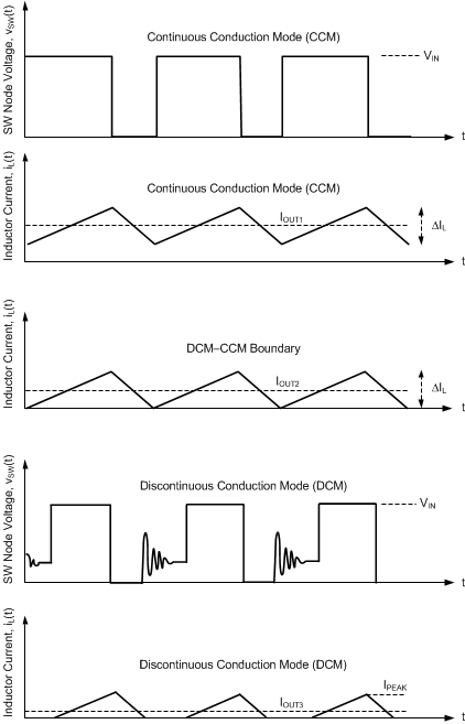
LM21215A CCM_DCM_nosb87.gifFigure 27. LM21215A Modes of Operation