SNOSB87D March 2011 – May 2019 LM21215A
PRODUCTION DATA.
- 1 Features
- 2 Applications
- 3 Description
- 4 Revision History
- 5 Pin Configuration and Functions
- 6 Specifications
- 7 Detailed Description
- 8 Application and Implementation
- 9 Power Supply Recommendations
- 10Layout
- 11Device and Documentation Support
- 12Mechanical, Packaging, and Orderable Information
Package Options
Mechanical Data (Package|Pins)
- PWP|20
Thermal pad, mechanical data (Package|Pins)
- PWP|20
Orderable Information
6.6 Typical Characteristics
Unless otherwise specified: VIN = 5 V, VOUT = 1.2 V, LF = 0.56 µH (1.8 mΩ RDCR), CSS = 33 nF, fSW = 500 kHz, TA = 25°C for efficiency curves, loop gain plots and waveforms, and TJ = 25°C for all others.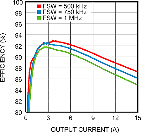 Figure 1. Efficiency
 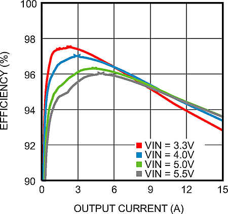 Figure 3. Efficiency (VOUT = 2.5 V, FSW= 500 kHz, Inductor P/N SER2010-601MLD)
 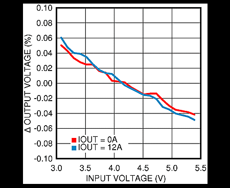 Figure 5. Line Regulation
 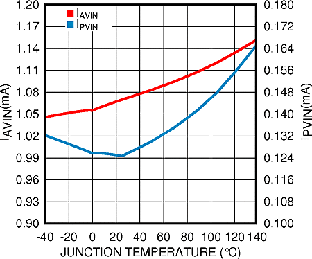 Figure 7. Non-Switching IAVIN and IPVIN vs Temperature
 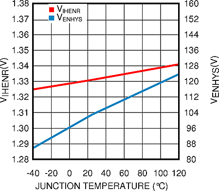 Figure 9. Enable Threshold and Hysteresis vs Temperature
 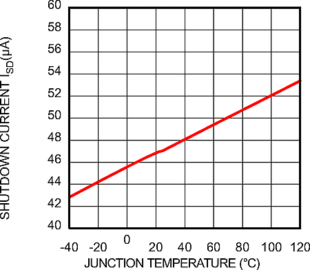 Figure 11. Enable Low Current vs Temperature
 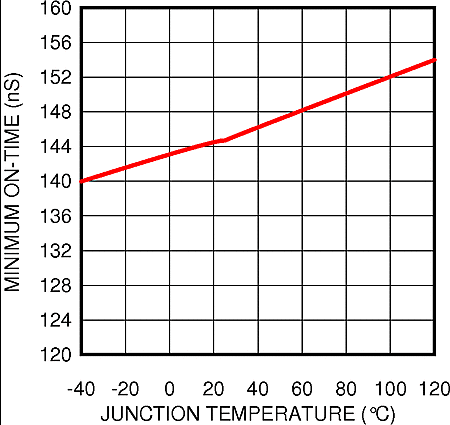 Figure 13. Minimum On-Time vs Temperature
 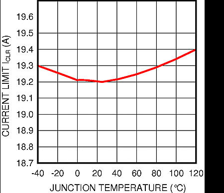 Figure 15. Peak Current Limit vs Temperature
 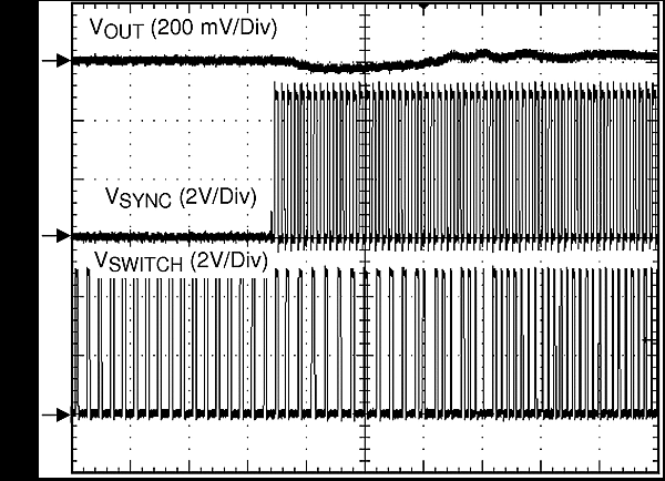 Figure 17. SYNC Signal Acquired, 10 µs/div
 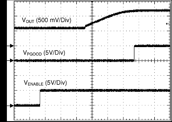 Figure 19. Startup with Prebiased Output, 2 ms/Div
 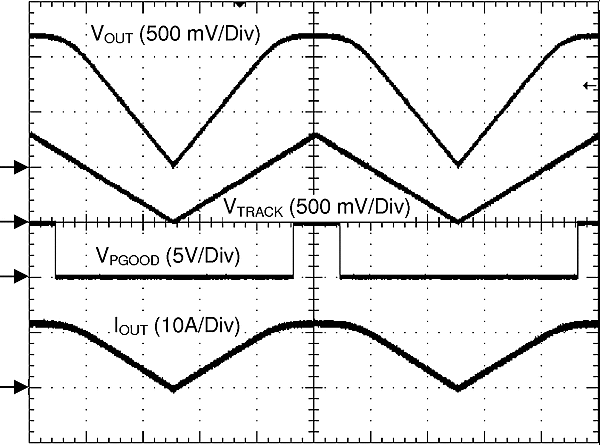 Figure 21. Startup with Tracking Signal Applied, 200 ms/Div
 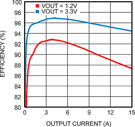 Figure 2. Efficiency
 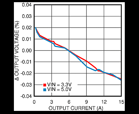 Figure 4. Load Regulation
 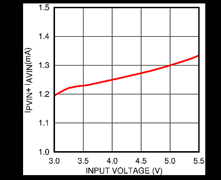 Figure 6. Non-Switching IQ(TOTAL) vs VIN
 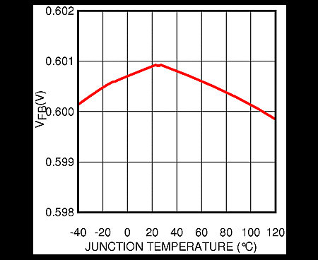 Figure 8. Feedback (FB) Voltage vs Temperature
 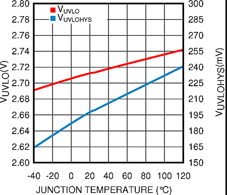 Figure 10. UVLO Threshold and Hysteresis vs Temperature
 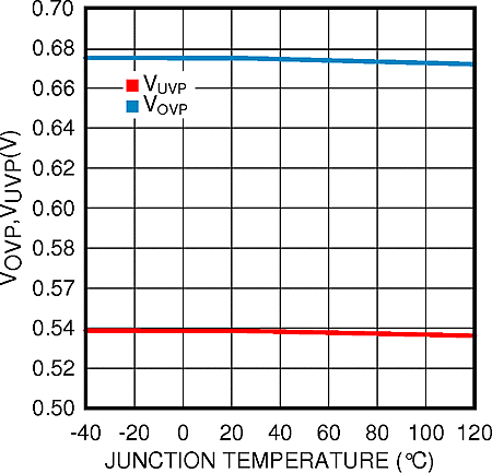 Figure 12. OVP/UVP Threshold vs Temperature
 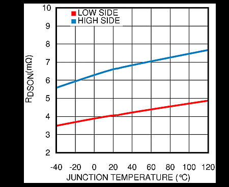 Figure 14. MOSFET On-State Resistance vs Temperature
 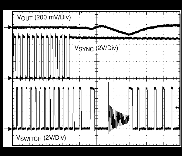 Figure 16. SYNC Signal Removed, 4 µs/Div
 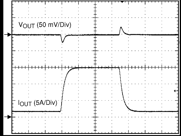 Figure 18. Load Transient Response, 100 µs/Div
 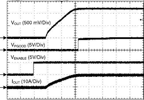 Figure 20. Startup with SS/TRK Open Circuit, 200 µs/Div
 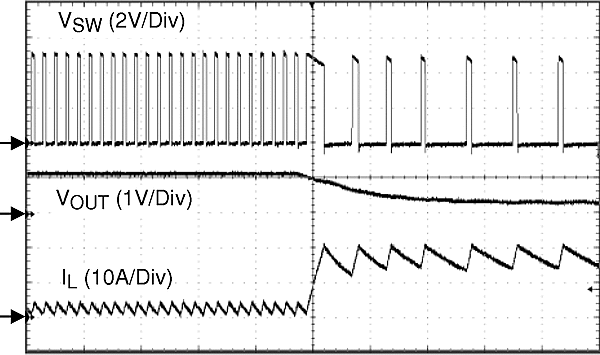 Figure 22. Output Overcurrent Condition, 10 µs/Div