SNVS639G December 2009 – December 2015 LM21305
PRODUCTION DATA.
- 1 Features
- 2 Applications
- 3 Description
- 4 Revision History
- 5 Description (continued)
- 6 Pin Configuration and Functions
- 7 Specifications
-
8 Detailed Description
- 8.1 Overview
- 8.2 Functional Block Diagram
- 8.3
Feature Description
- 8.3.1 Synchronous DC-DC Switching Converter
- 8.3.2 Peak Current-Mode Control
- 8.3.3 Switching Frequency Setting and Synchronization
- 8.3.4 Light-Load Operation
- 8.3.5 Precision Enable
- 8.3.6 Device Enable, Soft-Start, and Pre-Bias Startup Capability
- 8.3.7 Peak Current Protection and Negative Current Limiting
- 8.3.8 PGOOD Indicator
- 8.3.9 Internal Bias Regulators
- 8.3.10 Minimum On-Time Considerations
- 8.4 Device Functional Modes
-
9 Application and Implementation
- 9.1 Application Information
- 9.2
Typical Application
- 9.2.1 Design Requirements
- 9.2.2
Detailed Design Procedure
- 9.2.2.1 Setting the Output Voltage
- 9.2.2.2 Calculating the Duty Cycle
- 9.2.2.3 Input Capacitors
- 9.2.2.4 AVIN Filter
- 9.2.2.5 Switching Frequency Selection
- 9.2.2.6 Filter Inductor
- 9.2.2.7 Output Capacitor
- 9.2.2.8 Efficiency Considerations
- 9.2.2.9 Load Current Derating When Duty Cycle Exceeds 50%
- 9.2.2.10 Control Loop Compensation
- 9.2.2.11 Compensation Components Selection
- 9.2.2.12 Plotting the Loop Gain
- 9.2.2.13 High Frequency Considerations
- 9.2.2.14 Bootstrap Capacitor
- 9.2.2.15 5V0 and 2V5 Capacitors
- 9.2.2.16 Maximum Ambient Temperature
- 9.2.3 Application Curves
- 10Power Supply Recommendations
- 11Layout
- 12Device and Documentation Support
- 13Mechanical, Packaging, and Orderable Information
Package Options
Mechanical Data (Package|Pins)
- RSG|28
Thermal pad, mechanical data (Package|Pins)
Orderable Information
11 Layout
11.1 Layout Guidelines
PC board layout is an important and critical part of any dc-dc converter design. The performance of any switching converter depends as much upon the layout of the PCB as the component selection. Poor layout disrupts the performance of a dc-dc converter and surrounding circuitry by contributing to EMI, ground bounce, resistive voltage loss in the traces, and thermal problems. Erroneous signals can reach the dc-dc converter, possibly resulting in poor regulation or instability. There are several paths that conduct high slew-rate currents or voltages that can interact with stray inductance or parasitic capacitance to generate noise and EMI or degrade the power-supply performance.
The following guidelines serve to help users to design a PCB with the best power conversion performance, thermal performance, and minimized generation of unwanted EMI.
- Locate the input capacitors as close as possible to the PVIN and PGND pins, and place the inductor as close as possible to the SW pins and output capacitors. This placement is to minimize the area of switching current loops and reduce the resistive loss of the high current path. Based on the LM21305 pinout, place a 1-µF to 10-µF ceramic capacitor right by pins 1, 2, and 7, across the SW node trace, as an addition to the bulk input capacitors. Using a size 1206 or 1210 capacitor allows enough copper width for the SW node to be routed underneath the capacitor for good conduction (see the LM21305 evaluation board layout detailed in application note AN-2042 LM21305 Evaluation Board, SNVA432).
- Keep the SW node area small. Keep the copper area connecting the SW pin to the inductor as short and wide as possible. At the same time, minimize the total area of this node to help mitigate radiated EMI. Place the inductor as close as possible to the SW pins.
- Use a solid ground plane on layer two of the PCB, particularly underneath the LM21305 and power stage components. This plane functions as a noise shield and also as a heat dissipation path.
- Make input and output power bus connections as wide and short as possible to reduce any voltage drops on the input or output of the converter and to improve efficiency. Use copper planes on top to connect the multiple PVIN pins and PGND pins together.
- Provide enough PCB area for proper heat-sinking. As stated in the Maximum Ambient Temperature section, use enough copper area to ensure a low RθJA commensurate with the maximum load current and ambient temperature. Make the top and bottom PCB layers with two ounce copper and no less than one ounce. Use an array of heat-sinking vias to connect the exposed pad (DAP) to the ground plane on the bottom PCB layer. If the PCB has multiple copper layers (recommended), connect these thermal vias to the inner layer heat-spreading ground planes.
- Route the feedback trace from VOUT to the feedback divider resistors away from the SW pin and inductor to avoid contaminating this feedback signal with switching noise. This routing is most important when high resistances are used to set the output voltage. Routing the feedback trace on a different layer than the inductor and SW node trace is recommended such that a ground plane exists between the feedback trace and inductor or SW node polygon to provide further cancellation of EMI on the feedback trace.
- If voltage accuracy at the load is important, ensure that the feedback voltage sense is made directly at the load terminals. Doing so corrects for voltage drops in the PCB planes and traces and provides optimal output voltage setpoint accuracy and load regulation. Placing the resistor divider closer to the FB node, rather than close to the load, is always better because the FB node is the input to the error amplifier and is thus noise sensitive. COMP is a noise-sensitive node and the compensation components must be located as close as possible to the device.
- Use short, low-inductance traces for the CBOOT capacitor. Locate CBOOT as close as possible to the CBOOT and SW pins.
- Place the bypass capacitors for the 5V0 and 2V5 rails close to their respective pins.
- Place the frequency set resistor and its associated capacitor close to the FREQ pin.
- See PCB Layout Resources for additional guidelines.
11.1.1 Compact PCB Layout for EMI Reduction
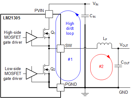
Radiated EMI generated by high di/dt components relates to pulsing currents in switching converters. The larger area covered by the path of a pulsing current, the more electromagnetic emission is generated. The key to minimize radiated EMI is to identify the pulsing current path and minimize the area of that path.
The main switching loop of the LM21305 power stage is denoted by #1 in Figure 37. The topological architecture of a buck converter means that particularly high di/dt current flows in loop #1, and it becomes mandatory to reduce the parasitic inductance of this loop by minimizing its effective loop area. For loop #2 however, the di/dt through inductor LF and capacitor COUT is naturally limited by the inductor. Keeping the area of loop #2 small is not nearly as important as that of loop #1. Also important are the gate drive loops of the low-side and high-side MOSFETs, which are inherently tight by virtue of the integrated power MOSFETs and gate drivers of the LM21305.
 Figure 37. DC-DC Buck Regulator with Power Stage Circuit Switching Loops
High-frequency ceramic bypass capacitors at the input side provide primary path for the high di/dt components of the pulsing current. Placing ceramic bypass capacitors as close as possible to the PVIN and PGND pins is the key to EMI reduction. Keep the SW trace connecting to the inductor as short as possible, and just wide enough to carry the load current without excessive heating. Use short, thick traces or copper pours (shapes) for current conduction path to minimize parasitic resistance. Place the output capacitors close to the VOUT side of the inductor and route the return using GND plane copper back to the LM21305 PGND pin and exposed PAD.
11.1.2 Ground Plane and Thermal Design Considerations
As mentioned previously, using one of the middle layers as a solid ground plane is recommended. A ground plane provides shielding for sensitive circuits and traces. This plane also provides a quiet reference potential for the control circuitry. Connect the AGND and PGND pins to the ground plane using vias right next to the bypass capacitors. The PGND pins are connected to the source of the internal low-side power MOSFET. Connect these pins directly to the return terminals of the input and output capacitors. The PGND net contains noise at the switching frequency and can bounce because of load variations. The PGND trace, as well as PVIN and SW traces, must be constrained to one side of the ground plane. The other side of the ground plane contains much less noise and can be used for sensitive routes.
Provide adequate device heat-sinking by using the exposed pad (DAP) of the LM21305 as the primary thermal path. Use a minimum 4-by-4 array of 10 mil thermal vias to connect the DAP to the system ground plane for heat-sinking. Evenly distribute the vias under the DAP. Use as much copper as possible for system ground plane on the top and bottom layers for best heat dissipation. A four-layer board with copper thickness, starting from the top, of 2 oz, 1 oz, 1 oz, 2 oz and with proper layout provides low impedance, proper shielding, and low thermal resistance. See Resources for Thermal PCB Design for additional thermal design guidelines.
11.2 Layout Example
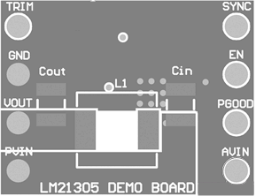
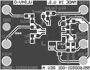
Figure 38 and Figure 39 show an example of an LM21305 PCB layout. Only the top and bottom layer copper and top silkscreen are shown. For more details, see application note AN-2175 LM21305 POL Demonstration Module and Reference Design, SNVA497.
 Figure 38. PCB Top Layer Copper and Silkscreen
 Figure 39. PCB Bottom Layer Copper and Silkscreen