SLOS066AD September 1975 – October 2024 LM124 , LM124A , LM224 , LM224A , LM224K , LM224KA , LM2902 , LM2902B , LM2902BA , LM2902K , LM2902KAV , LM2902KV , LM324 , LM324A , LM324B , LM324BA , LM324K , LM324KA
PRODUCTION DATA
- 1
- 1 Features
- 2 Applications
- 3 Description
- 4 Pin Configuration and Functions
-
5 Specifications
- 5.1 Absolute Maximum Ratings
- 5.2 ESD Ratings
- 5.3 Recommended Operating Conditions
- 5.4 Thermal Information
- 5.5 Electrical Characteristics - LM324B and LM324BA
- 5.6 Electrical Characteristics - LM2902B and LM2902BA
- 5.7 Electrical Characteristics for LM324, LM324K, LM224, LM224K, and LM124
- 5.8 Electrical Characteristics for LM2902, LM2902K, LM2902KV and LM2902KAV
- 5.9 Electrical Characteristics for LM324A, LM324KA, LM224A, LM224KA, and LM124A
- 5.10 Operating Conditions
- 5.11 Typical Characteristics
- 5.12 Typical Characteristics: All Devices Except B and BA Versions
- 6 Parameter Measurement Information
- 7 Detailed Description
- 8 Application and Implementation
- 9 Device and Documentation Support
- 10Revision History
- 11Mechanical, Packaging, and Orderable Information
Package Options
Refer to the PDF data sheet for device specific package drawings
Mechanical Data (Package|Pins)
- D|14
- N|14
Thermal pad, mechanical data (Package|Pins)
Orderable Information
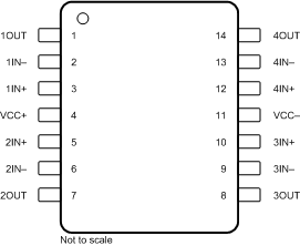
4 Pin Configuration and Functions
 Figure 4-1 D, DB, J, N, NS, PW, and W Packages,
14-Pin SOIC, SSOP, CDIP, PDIP, SO, TSSOP, and CFP
(Top View)

| NOTE: RTE package is preview only |
16-Pin WQFN
(Top View)
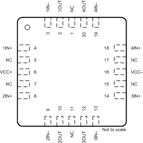
 Figure 4-2 FK Package,
20-Pin LCCC
(Top View)
Table 4-1 Pin Functions
| PIN | TYPE(1) | DESCRIPTION | |||
|---|---|---|---|---|---|
| NAME | LCCC | SOIC, TSSOP, PDIP, SSOP, SO, CDIP, and CFP | WQFN | ||
| 1IN– | 3 | 2 | 16 | I | Negative input |
| 1IN+ | 4 | 3 | 1 | I | Positive input |
| 1OUT | 2 | 1 | 15 | O | Output |
| 2IN– | 9 | 6 | 5 | I | Negative input |
| 2IN+ | 8 | 5 | 4 | I | Positive input |
| 2OUT | 10 | 7 | 6 | O | Output |
| 3IN– | 13 | 9 | 8 | I | Negative input |
| 3IN+ | 14 | 10 | 9 | I | Positive input |
| 3OUT | 12 | 8 | 7 | O | Output |
| 4IN– | 19 | 13 | 13 | I | Negative input |
| 4IN+ | 18 | 12 | 12 | I | Positive input |
| 4OUT | 20 | 14 | 14 | O | Output |
| VCC- | 16 | 11 | 11 | — | Negative (lowest) supply or ground (for single-supply operation) |
| NC | 1, 5, 7, 11, 15, 17 | — | 3, 10 | — | Do not connect |
| VCC+ | 6 | 4 | 2 | — | Positive (highest) supply |
(1) I = input, O = output