LM22672/-Q1 42-V, 1-A SIMPLE SWITCHER® Step-Down Voltage Regulator with Features
1 Features
- Wide Input Voltage Range: 4.5 V to 42 V
- Internally Compensated Voltage Mode Control
- Stable with Low ESR Ceramic Capacitors
- 200 mΩ N-Channel MOSFET
- Output Voltage Options:
-ADJ (Outputs as Low as 1.285 V)
-5.0 (Output Fixed to 5 V) - ±1.5% Feedback Reference Accuracy
- 500 kHz Default Switching Frequency
- Adjustable Switching Frequency and Synchronization
- –40°C to 125°C Junction Temperature Range
- Precision Enable Input
- Integrated Boot-Strap Diode
- Adjustable Soft-Start
- Fully WEBENCH® Enabled
- LM22672-Q1 is an Automotive Grade Product
that is AEC-Q100 Grade 1 Qualified (–40°C to +125°C Junction Temperature) - SO PowerPAD (Exposed Pad)
2 Applications
- Industrial Control
- Telecom and Datacom Systems
- Embedded Systems
- Conversions from Standard 24 V, 12 V and 5 V Input Rails
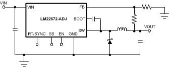
Simplified Application Schematic
3 Description
The LM22672 switching regulator provides all of the functions necessary to implement an efficient high voltage step-down (buck) regulator using a minimum of external components. This easy to use regulator incorporates a 42 V N-channel MOSFET switch capable of providing up to 1 A of load current. Excellent line and load regulation along with high efficiency (> 90%) are featured. Voltage mode control offers short minimum on-time, allowing the widest ratio between input and output voltages. Internal loop compensation means that the user is free from the tedious task of calculating the loop compensation components. Fixed 5 V output and adjustable output voltage options are available.
The default switching frequency is set at 500 kHz allowing for small external components and good transient response. In addition, the frequency can be adjusted over a range of 200 kHz to 1 MHz with a single external resistor. The internal oscillator can be synchronized to a system clock or to the oscillator of another regulator. A precision enable input allows simplification of regulator control and system power sequencing. In shutdown mode the regulator draws only 25 µA (typ). An adjustable soft-start feature is provided through the selection of a single external capacitor. The LM22672 also has built in thermal shutdown, and current limiting to protect against accidental overloads.
The LM22672 is a member of Texas Instruments' SIMPLE SWITCHER® family. The SIMPLE SWITCHER® concept provides for an easy to use complete design using a minimum number of external components and the TI WEBENCH® design tool. TI's WEBENCH® tool includes features such as external component calculation, electrical simulation, thermal simulation, and Build-It boards for easy design-in.
Device Information(1)
| PART NUMBER | PACKAGE | BODY SIZE (NOM) |
|---|---|---|
| LM22672, LM22672-Q1 |
HSOP (8) | 4.89 mm x 3.90 mm |
- For all available packages, see the orderable addendum at the end of the data sheet.
4 Revision History
Changes from L Revision (April 2013) to M Revision
- Added Pin Configuration and Functions section, Handling Rating table, Feature Description section, Device Functional Modes, Application and Implementation section, Power Supply Recommendations section, Layout section, Device and Documentation Support section, and Mechanical, Packaging, and Orderable Information section Go
Changes from K Revision (April 2013) to L Revision
- Changed from National to TI format Go
5 Pin Configuration and Functions

Pin Functions
| PIN | TYPE | DESCRIPTION | APPLICATION INFORMATION | |
|---|---|---|---|---|
| NAME | NO. | |||
| BOOT | 1 | I | Bootstrap input | Provides the gate voltage for the high side NFET. |
| EN | 5 | I | Enable input | Used to control regulator start-up and shutdown. See Precision Enable and UVLO section of data sheet. |
| EP | EP | — | Exposed Pad | Connect to ground. Provides thermal connection to PCB. See Thermal Considerations. |
| FB | 4 | I | Feedback input | Feedback input to regulator. |
| GND | 6 | — | Ground input to regulator; system common |
System ground pin. |
| RT/SYNC | Oscillator mode control input | Used to control oscillator mode of regulator. See Switching Frequency Adjustment and Synchronization section of data sheet. | ||
| SS | 2 | I | Soft-start input | Used to increase soft-start time. See Soft-Start section of data sheet. |
| SW | 8 | O | Switch output | Switching output of regulator. |
| VIN | I | Input voltage | Supply input to the regulator. | |
6 Specifications
6.1 Absolute Maximum Ratings(1)(2)
over operating free-air temperature range (unless otherwise noted)| MIN | MAX | UNIT | ||
|---|---|---|---|---|
| VIN to GND | 43 | V | ||
| EN Pin Voltage | –0.5 | 6 | V | |
| SS, RT/SYNC Pin Voltage | –0.5 | 7 | V | |
| SW to GND(3) | –5 | VIN | V | |
| BOOT Pin Voltage | VSW + 7 | V | ||
| FB Pin Voltage | –0.5 | 7 | V | |
| Power Dissipation | Internally Limited | |||
| Junction Temperature | 150 | °C | ||
| For soldering specifications, refer to Application Report Absolute Maximum Ratings for Soldering (SNOA549). | ||||
6.2 Handling Ratings: LM22672
| MIN | MAX | UNIT | |||
|---|---|---|---|---|---|
| Tstg | Storage temperature range | –65 | 150 | °C | |
| V(ESD) | Electrostatic discharge | Human body model (HBM), per ANSI/ESDA/JEDEC JS-001, all pins(1) | –2 | 2 | kV |
6.3 Handling Ratings: LM22672-Q1
| MIN | MAX | UNIT | ||||
|---|---|---|---|---|---|---|
| Tstg | Storage temperature range | –65 | 150 | °C | ||
| V(ESD) | Electrostatic discharge | Human body model (HBM), per AEC Q100-002(1) | –2 | 2 | kV | |
6.4 Recommended Operating Conditions
| MIN | MAX | UNIT | ||
|---|---|---|---|---|
| VIN | Supply Voltage | 4.5 | 42 | V |
| Junction Temperature Range | –40 | 125 | °C | |
6.5 Thermal Information
| THERMAL METRIC(1) | LM22672, LM22672-Q1 | UNIT | |||
|---|---|---|---|---|---|
| HSOP | |||||
| 8 PINS | |||||
| RθJA | Junction-to-ambient thermal resistance | MR Package, Junction to ambient thermal resistance(2) | 60 | °C/W | |
6.6 Electrical Characteristics
Typical values represent the most likely parametric norm at TA = TJ = 25°C, and are provided for reference purposes only. Unless otherwise specified: VIN = 12 V.| PARAMETER | TEST CONDITIONS | MIN(5) | TYP(4) | MAX(5) | UNIT | |
|---|---|---|---|---|---|---|
| LM22672-5.0 | ||||||
| VFB | Feedback Voltage | VIN = 8 V to 42 V | 4.925 | 5.0 | 5.075 | V |
| VIN = 8 V to 42 V, –40°C ≤ TJ ≤ 125°C | 4.9 | 5.1 | ||||
| LM22672-ADJ | ||||||
| VFB | Feedback Voltage | VIN = 4.7 V to 42 V | 1.266 | 1.285 | 1.304 | V |
| VIN = 4.7 V to 42 V, –40°C ≤ TJ ≤ 125°C | 1.259 | 1.311 | ||||
| ALL OUTPUT VOLTAGE VERSIONS | ||||||
| IQ | Quiescent Current | VFB = 5 V | 3.4 | mA | ||
| VFB = 5 V, –40°C ≤ TJ ≤ 125°C | 6 | |||||
| ISTDBY | Standby Quiescent Current | EN Pin = 0 V | 25 | 40 | µA | |
| ICL | Current Limit | 1.3 | 1.5 | 1.7 | A | |
| –40°C ≤ TJ ≤ 125°C | 1.2 | 1.8 | ||||
| IL | Output Leakage Current | VIN = 42 V, EN Pin = 0 V, VSW = 0 V | 0.2 | 2 | µA | |
| VSW = –1 V | 0.1 | 3 | µA | |||
| RDS(ON) | Switch On-Resistance | 0.2 | 0.24 | Ω | ||
| –40°C ≤ TJ ≤ 125°C | 0.32 | |||||
| Fsw | Oscillator Frequency | 500 | kHz | |||
| –40°C ≤ TJ ≤ 125°C | 400 | 600 | ||||
| TOFF | Minimum Off-time | 200 | ns | |||
| –40°C ≤ TJ ≤ 125°C | 100 | 300 | ||||
| TON | Minimum On-time | 100 | ns | |||
| IBIAS | Feedback Bias Current | VFB = 1.3 V (ADJ Version Only) | 230 | nA | ||
| VEN | Enable Threshold Voltage | Falling | 1.6 | V | ||
| Falling, –40°C ≤ TJ ≤ 125°C | 1.3 | 1.9 | ||||
| VENHYST | Enable Voltage Hysteresis | 0.6 | V | |||
| IEN | Enable Input Current | EN Input = 0 V | 6 | µA | ||
| FSYNC | Maximum Synchronization Frequency | VSYNC = 3.5 V, 50% duty-cycle | 1 | MHz | ||
| VSYNC | Synchronization Threshold Voltage | 1.75 | V | |||
| ISS | Soft-Start Current | 50 | µA | |||
| –40°C ≤ TJ ≤ 125°C | 30 | 70 | ||||
| TSD | Thermal Shutdown Threshold | 150 | °C | |||
6.7 Typical Characteristics
Vin = 12 V, TJ = 25°C (unless otherwise specified) Figure 1. Efficiency vs IOUT and VIN, VOUT = 3.3 V
 Figure 3. Current Limit vs Temperature
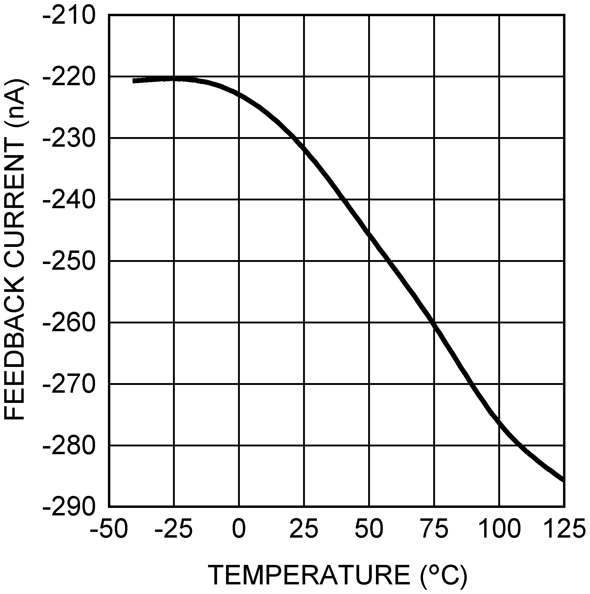 Figure 5. Feedback Bias Current vs Temperature
 Figure 7. Standby Quiescent Current vs Input Voltage
 Figure 9. Normalized Feedback Voltage vs Input Voltage
 Figure 11. Soft-Start Current vs Temperature
 Figure 2. Normalized Switching Frequency vs Temperature
 Figure 4. Normalized RDS(ON) vs Temperature
 Figure 6. Normalized Enable Threshold Voltage vs Temperature
 Figure 8. Normalized Feedback Voltage vs Temperature
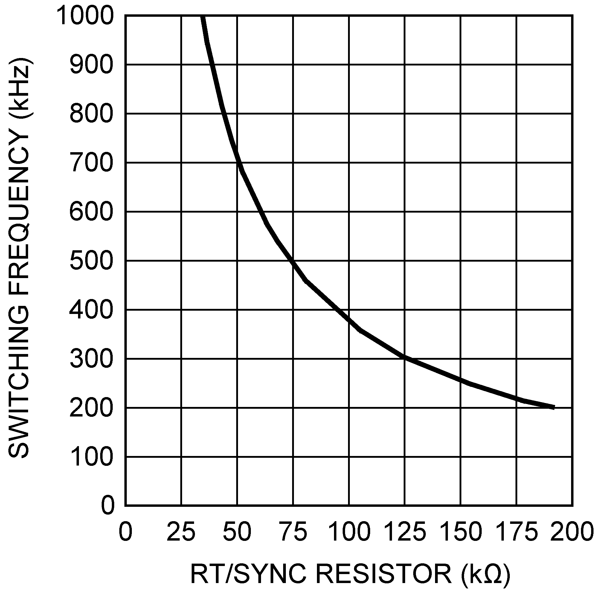 Figure 10. Switching Frequency vs RT/SYNC Resistor
7 Detailed Description
7.1 Overview
The LM22672 device incorporates a voltage mode constant frequency PWM architecture. In addition, input voltage feedforward is used to stabilize the loop gain against variations in input voltage. This allows the loop compensation to be optimized for transient performance. The power MOSFET, in conjunction with the diode, produce a rectangular waveform at the switch pin that swings from about zero volts to VIN. The inductor and output capacitor average this waveform to become the regulator output voltage. By adjusting the duty cycle of this waveform, the output voltage can be controlled. The error amplifier compares the output voltage with the internal reference and adjusts the duty cycle to regulate the output at the desired value.
The internal loop compensation of the -ADJ option is optimized for outputs of 5 V and below. If an output voltage of 5 V or greater is required, the -5.0 option can be used with an external voltage divider. The minimum output voltage is equal to the reference voltage, that is, 1.285 V (typ).
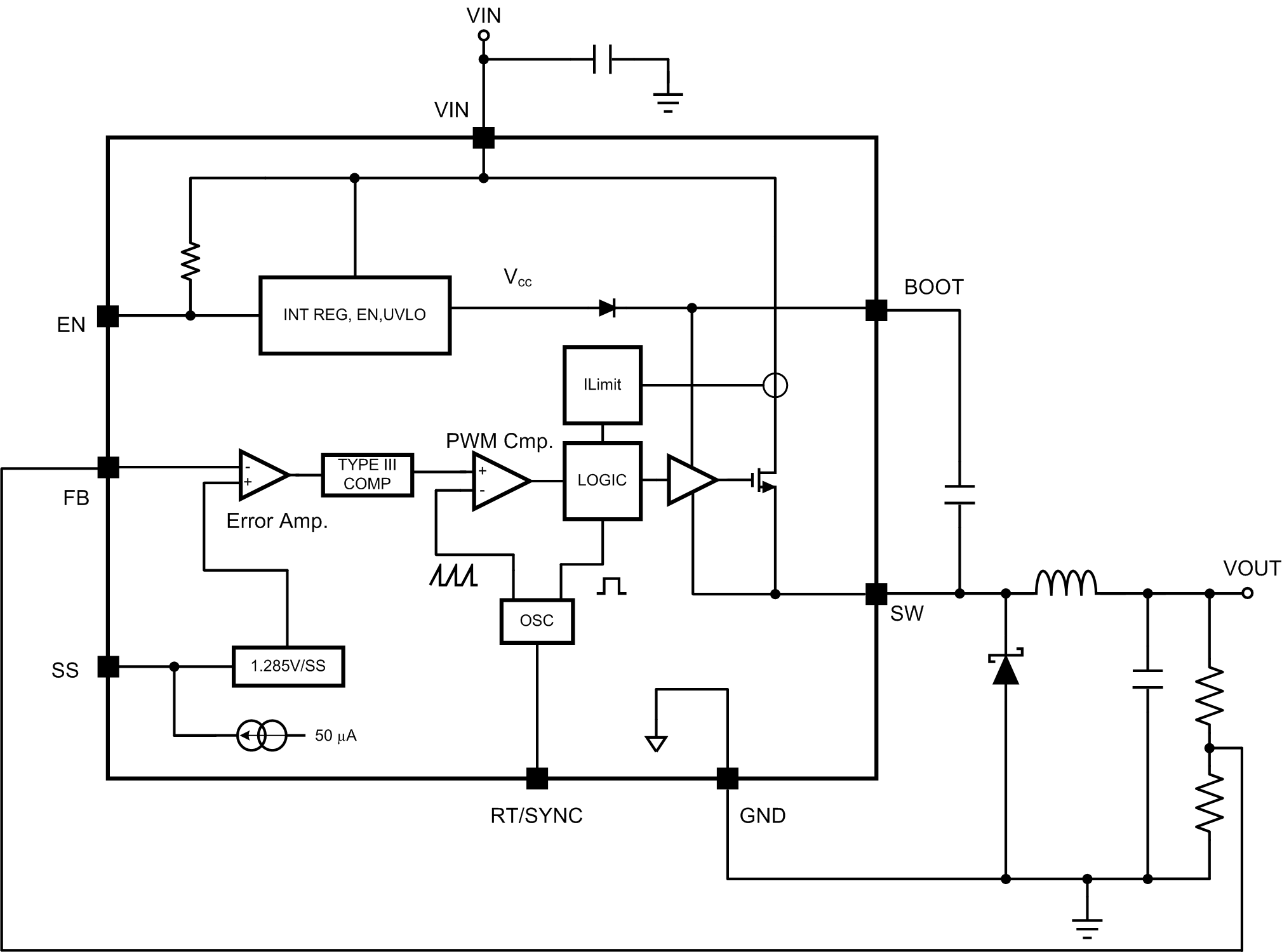
7.2 Functional Block Diagram
7.3 Feature Description
7.3.1 Precision Enable and UVLO
The precision enable input (EN) is used to control the regulator. The precision feature allows simple sequencing of multiple power supplies with a resistor divider from another supply. Connecting this pin to ground or to a voltage less than 1.6 V (typ) will turn off the regulator. The current drain from the input supply, in this state, is 25 µA (typ) at an input voltage of 12 V. The EN input has an internal pullup of about 6 µA. Therefore this pin can be left floating or pulled to a voltage greater than 2.2 V (typ) to turn the regulator on. The hysteresis on this input is about 0.6 V (typ) above the 1.6-V (typ) threshold. When driving the enable input, the voltage must never exceed the 6 V absolute maximum specification for this pin.
Although an internal pullup is provided on the EN pin, it is good practice to pull the input high, when this feature is not used, especially in noisy environments. This can most easily be done by connecting a resistor between VIN and the EN pin. The resistor is required, because the internal zener diode, at the EN pin, will conduct for voltages above about 6 V. The current in this zener must be limited to less than 100 µA. A resistor of 470 kΩ will limit the current to a safe value for input voltages as high 42 V. Smaller values of resistor can be used at lower input voltages.
The LM22672 device also incorporates an input undervoltage lock-out (UVLO) feature. This prevents the regulator from turning on when the input voltage is not great enough to properly bias the internal circuitry. The rising threshold is 4.3 V (typ) while the falling threshold is 3.9 V (typ). In some cases these thresholds may be too low to provide good system performance. The solution is to use the EN input as an external UVLO to disable the part when the input voltage falls below a lower boundary. This is often used to prevent excessive battery discharge or early turn-on during start-up. This method is also recommended to prevent abnormal device operation in applications where the input voltage falls below the minimum of 4.5 V. Figure 12 shows the connections to implement this method of UVLO. Equation 1 and Equation 2 can be used to determine the correct resistor values.
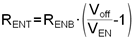
Where:
Voff is the input voltage where the regulator shuts off.
Von is the voltage where the regulator turns on.
Due to the 6 µA pullup, the current in the divider should be much larger than this. A value of 20 kΩ, for RENB is a good first choice. Also, a zener diode may be needed between the EN pin and ground in order to comply with the absolute maximum ratings on this pin.
 Figure 12. External UVLO Connections
7.3.2 Soft-Start
The soft-start feature allows the regulator to gradually reach steady-state operation, thus reducing start-up stresses. The internal soft-start feature brings the output voltage up in about 500 µs. This time can be extended by using an external capacitor connected to the SS pin. Values in the range of 100 nF to 1 µF are recommended. The approximate soft-start time can be estimated from Equation 3.

Soft-start is reset any time the part is shut down or a thermal overload event occurs.
7.3.3 Switching Frequency Adjustment and Synchronization
The LM22672 device will operate in three different modes, depending on the condition of the RT/SYNC pin. With the RT/SYNC pin floating, the regulator will switch at the internally set frequency of 500 kHz (typ). With a resistor in the range of 25 kΩ to 200 kΩ, connected from RT/SYNC to ground, the internal switching frequency can be adjusted from 1 MHz to 200 kHz. Figure 13 shows the typical curve for switching frequency versus the external resistance connected to the RT/SYNC pin. The accuracy of the switching frequency, in this mode, is slightly worse than that of the internal oscillator; about ±25% is to be expected. Finally, an external clock can be applied to the RT/SYNC pin to allow the regulator to synchronize to a system clock or another LM22672. The mode is set during start up of the regulator. When the LM22672 is enabled, or after VIN is applied, a weak pullup is connected to the RT/SYNC pin and, after approximately 100 µs, the voltage on the pin is checked against a threshold of about 0.8 V. With the RT/SYNC pin open, the voltage floats above this threshold, and the mode is set to run with the internal clock. With a frequency set resistor present, an internal reference holds the pin voltage at 0.8 V; thus, the resulting current sets the mode to allow the resistor to control the clock frequency. If the external circuit forces the RT/SYNC pin to a voltage much greater or less than 0.8 V, the mode is set to allow external synchronization. The mode is latched until either the EN or the input supply is cycled.
The choice of switching frequency is governed by several considerations. As an example, lower frequencies may be desirable to reduce switching losses or improve duty cycle limits. Higher frequencies, or a specific frequency, may be desirable to avoid problems with EMI or reduce the physical size of external components. The flexibility of increasing the switching frequency above 500 kHz can also be used to operate outside a critical signal frequency band for a given application. Keep in mind that the values of inductor and output capacitor cannot be reduced dramatically by operating above 500 kHz. This is true because the design of the internal loop compensation restricts the range of these components.
Frequency synchronization requires some care. First the external clock frequency must be greater than the internal clock frequency, and less than 1 MHz. The maximum internal switching frequency is ensured in the Electrical Characteristics table.
NOTE
The frequency adjust feature and the synchronization feature can not be used simultaneously.
The synchronizing frequency must always be greater than the internal clock frequency. Secondly, the RT/SYNC pin must see a valid high or low voltage, during start-up, in order for the regulator to go into the synchronizing mode. Also, the amplitude of the synchronizing pulses must comport with VSYNC levels found in the Electrical Characteristics table. The regulator will synchronize on the rising edge of the external clock. If the external clock is lost during normal operation, the regulator will revert to the 500 kHz (typ) internal clock.
If the frequency synchronization feature is used, current limit foldback is not operational; see the Current Limit section for details.
Figure 13. Switching Frequency vs RT/SYNC Resistor
7.3.4 Self-Synchronization
It is possible to synchronize multiple LM22672 regulators together to share the same switching frequency. This can be done by tying the RT/SYNC pins together through a MOSFET and connecting a 1 kΩ resistor to ground at each pin. Figure 14 shows this connection. The gate of the MOSFET should be connected to the regulator with the highest output voltage. Also, the EN pins of both regulators should be tied to the common system enable, in order to properly initialize both regulators. The operation is as follows: When the regulators are enabled, the outputs are low and the MOSFET is off. The 1 kΩ resistors pull the RT/SYNC pins low, thus enabling the synchronization mode. These resistors are small enough to pull the RT/SYNC pin low, rather than activate the frequency adjust mode. Once the output voltage of one of the regulators is sufficient to turn on the MOSFET, the two RT/SYNC pins are tied together and the regulators will run in synchronized mode. The two regulators will be clocked at the same frequency but slightly phase shifted according to the minimum off-time of the regulator with the fastest internal oscillator. The slight phase shift helps to reduce stress on the input capacitors of the regulator. It is important to choose a MOSFET with a low gate threshold voltage so that the MOSFET will be fully enhanced. Also, a MOSFET with low inter-electrode capacitance is required. The 2N7002 is a good choice.
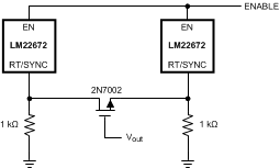 Figure 14. Self-Synchronizing Setup
7.3.5 Boot-Strap Supply
The LM22672 incorporates a floating high-side gate driver to control the power MOSFET. The supply for this driver is the external boot-strap capacitor connected between the BOOT pin and SW. A good quality 10 nF ceramic capacitor must be connected to these pins with short, wide PCB traces. One reason the regulator imposes a minimum off-time is to ensure that this capacitor recharges every switching cycle. A minimum load of about 5 mA is required to fully recharge the boot-strap capacitor in the minimum off-time. Some of this load can be provided by the output voltage divider, if used.
7.3.6 Internal Loop Compensation
The LM22672 device has internal loop compensation designed to provide a stable regulator over a wide range of external power stage components. The internal compensation of the -ADJ option is optimized for output voltages below 5 V. If an output voltage of 5 V or greater is needed, the -5.0 option with an external resistor divider can be used.
Ensuring stability of a design with a specific power stage (inductor and output capacitor) can be tricky. The LM22672 stability can be verified using the WEBENCH Designer online circuit simulation tool. A quick start spreadsheet can also be downloaded from the online product folder.
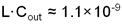
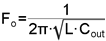
The complete transfer function for the regulator loop is found by combining the compensation and power stage transfer functions. The LM22672 has internal type III loop compensation, as detailed in Figure 15. This is the approximate "straight line" function from the FB pin to the input of the PWM modulator. The power stage transfer function consists of a dc gain and a second order pole created by the inductor and output capacitor(s). Due to the input voltage feedforward employed in the LM22672, the power stage dc gain is fixed at 20 dB. The second order pole is characterized by its resonant frequency and its quality factor (Q). For a first pass design, the product of inductance and output capacitance should conform to Equation 4.
Alternatively, this pole should be placed between 1.5 kHz and 15 kHz and is given by Equation 5.
The Q factor depends on the parasitic resistance of the power stage components and is not typically in the control of the designer. Of course, loop compensation is only one consideration when selecting power stage components; see the Application Information section for more details.
 Figure 15. Compensator Gain
In general, hand calculations or simulations can only aid in selecting good power stage components. Good design practice dictates that load and line transient testing should be done to verify the stability of the application. Also, Bode plot measurements should be made to determine stability margins. AN-1889 How to Measure the Loop Transfer Function of Power Supplies (SNVA364) shows how to perform a loop transfer function measurement with only an oscilloscope and function generator.
7.4 Device Functional Mode
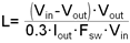
7.4.1 Current Limit
The LM22672 device has current limiting to prevent the switch current from exceeding safe values during an accidental overload on the output. This peak current limit is found in the Electrical Characteristics table under the heading of ICL. The maximum load current that can be provided, before current limit is reached, is determined from Equation 6.
Where:
L is the value of the power inductor.
When the LM22672 device enters current limit, the output voltage will drop and the peak inductor current will be fixed at ICL at the end of each cycle. The switching frequency will remain constant while the duty cycle drops. The load current will not remain constant, but will depend on the severity of the overload and the output voltage.
For very severe overloads ("short-circuit"), the regulator changes to a low frequency current foldback mode of operation. The frequency foldback is about 1/5 of the nominal switching frequency. This will occur when the current limit trips before the minimum on-time has elapsed. This mode of operation is used to prevent inductor current "run-away", and is associated with very low output voltages when in overload. Equation 7 can be used to determine what level of output voltage will cause the part to change to low frequency current foldback.
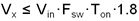
Where:
Fsw is the normal switching frequency.
Vin is the maximum for the application.
If the overload drives the output voltage to less than or equal to Vx, the part will enter current foldback mode. If a given application can drive the output voltage to ≤ Vx during an overload, then a second criterion must be checked. Equation 8 gives the maximum input voltage, when in this mode, before damage occurs.
Where:
Vsc is the value of output voltage during the overload.
Fsw is the normal switching frequency.
NOTE
If the input voltage should exceed this value, while in foldback mode, the regulator and/or the diode may be damaged.
It is important to note that the voltages in these equations are measured at the inductor. Normal trace and wiring resistance will cause the voltage at the inductor to be higher than that at a remote load. Therefore, even if the load is shorted with zero volts across its terminals, the inductor will still see a finite voltage. It is this value that should be used for Vx and Vsc in the calculations. In order to return from foldback mode, the load must be reduced to a value much lower than that required to initiate foldback. This load "hysteresis" is a normal aspect of any type of current limit foldback associated with voltage regulators.
If the frequency synchronization feature is used, the current limit frequency foldback is not operational, and the system may not survive a hard short-circuit at the output.
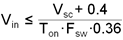
The safe operating areas, when in short circuit mode, are shown in Figure 16 through Figure 18 for different switching frequencies. Operating points below and to the right of the curve represent safe operation.
NOTE
The curves shown in Figure 16, Figure 17, and Figure 18 are not valid when the LM22672 is in frequency synchronization mode.
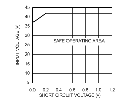 Figure 16. SOA at 300 kHz
 Figure 18. SOA at 800 kHz
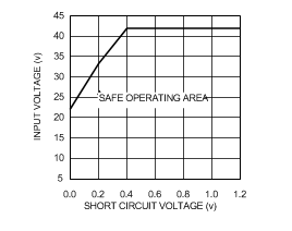 Figure 17. SOA at 500 kHz
7.4.2 Thermal Protection
Internal thermal shutdown circuitry protects the LM22672 should the maximum junction temperature be exceeded. This protection is activated at about 150°C, with the result that the regulator will shutdown until the temperature drops below about 135°C.
7.4.3 Duty-Cycle Limits
Ideally the regulator would control the duty cycle over the full range of zero to one. However due to inherent delays in the circuitry, there are limits on both the maximum and minimum duty cycles that can be reliably controlled. This in turn places limits on the maximum and minimum input and output voltages that can be converted by the LM22672. A minimum on-time is imposed by the regulator in order to correctly measure the switch current during a current limit event. A minimum off-time is imposed in order the re-charge the bootstrap capacitor. Equation 9 can be used to determine the approximate maximum input voltage for a given output voltage.
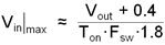
Where:
Fsw is the switching frequency.
TON is the minimum on-time.
Both parameters can be found in the Electrical Characteristics table.
If the frequency adjust feature is used, that value should be used for Fsw. Nominal values should be used. The worst case is lowest output voltage and highest switching frequency. If this input voltage is exceeded, the regulator will skip cycles, effectively lowering the switching frequency. The consequences of this are higher output voltage ripple and a degradation of the output voltage accuracy.
The second limitation is the maximum duty cycle before the output voltage will "dropout" of regulation. Equation 10 can be used to approximate the minimum input voltage before dropout occurs.

Where:
The values of TOFF and RDS(ON) are found in the Electrical Characteristics table.
The worst case here is highest switching frequency and highest load. In this equation, RL is the dc inductor resistance. Of course, the lowest input voltage to the regulator must not be less than 4.5 V (typ).
8 Application and Implementation
NOTE
Information in the following applications sections is not part of the TI component specification, and TI does not warrant its accuracy or completeness. TI’s customers are responsible for determining suitability of components for their purposes. Customers should validate and test their design implementation to confirm system functionality.
8.1 Application Information
The LM22672 device is a step down dc-to-dc regulator. It is typically used to convert a higher dc voltage to a lower dc voltage with a maximum output current of 1 A. Detailed Design Procedure can be used to select components for the LM22670 device. Alternately, the WEBENCH® software may be used to generate complete designs. When generating a design, the WEBENCH® software utilizes iterative design procedure and accesses comprehensive databases of components. Go to WEBENCH Designer for more details. This section presents a simplified discussion of the design process.
8.1.1 Output Voltage Divider Selection
For output voltages between about 1.285 V and 5 V, the -ADJ option should be used, with an appropriate voltage divider as shown in Figure 19. Equation 11 can be used to calculate the resistor values of this divider:

A good value for RFBB is 1k Ω. This will help to provide some of the minimum load current requirement and reduce susceptibility to noise pick-up. The top of RFBT should be connected directly to the output capacitor or to the load for remote sensing. If the divider is connected to the load, a local high-frequency bypass should be provided at that location.
For output voltages of 5 V, the -5.0 option should be used. In this case no divider is needed and the FB pin is connected to the output. The approximate values of the internal voltage divider are as follows: 7.38k from the FB pin to the input of the error amplifier and 2.55k from there to ground.
Both the -ADJ and -5.0 options can be used for output voltages greater than 5 V, by using the correct output divider. As mentioned in the Internal Loop Compensation section, the -5.0 option is optimized for output voltages of 5 V. However, for output voltages greater than 5 V, this option may provide better loop bandwidth than the -ADJ option, in some applications. If the -5.0 option is to be used at output voltages greater than 5 V, Equation 12 should be used to determine the resistor values in the output divider:

Again a value of RFBB of about 1k Ω is a good first choice.
 Figure 19. Output Voltage Divider
A maximum value of 10 kΩ is recommended for the sum of RFBB and RFBT to maintain good output voltage accuracy for the -ADJ option. A maximum of 2 kΩ is recommended for the -5.0 option. For the -5.0 option, the total internal divider resistance is typically 9.93 kΩ.
In all cases the output voltage divider should be placed as close as possible to the FB pin of the LM22672; because this is a high impedance input and is susceptible to noise pick-up.
8.1.2 Power Diode
A Schottky type power diode is required for all LM22672 applications. Ultra-fast diodes are not recommended and may result in damage to the IC due to reverse recovery current transients. The near ideal reverse recovery characteristics and low forward voltage drop of Schottky diodes are particularly important for high input voltage and low output voltage applications common to the LM22672. The reverse breakdown rating of the diode should be selected for the maximum VIN, plus some safety margin. A good rule of thumb is to select a diode with a reverse voltage rating of 1.3 times the maximum input voltage.
Select a diode with an average current rating at least equal to the maximum load current that will be seen in the application.
8.2 Typical Application
8.2.1 Typical Buck Regulator Application
Figure 20 shows an example of converting an input voltage range of 5.5 V to 35 V, to an output of 3.3 V at 1 Amp.
 Figure 20. Typical Buck Regulator Application
8.2.1.1 Design Requirements
| DESIGN PARAMETERS | EXAMPLE VALUE |
|---|---|
| Driver Supply Voltage (VIN) | 4.5 to 42 V |
| Output Voltage (VOUT) | 3.3 V |
| RFBT | Calculated based on RFBB and VREF of 1.285 V. |
| RFBB | 1 kΩ to 10 kΩ |
| IOUT | 3 A |
8.2.1.2 Detailed Design Procedure
8.2.1.2.1 External Components
The following guidelines should be used when designing a step-down (buck) converter with the LM22672.
8.2.1.2.1.1 Inductor
The inductor value is determined based on the load current, ripple current, and the minimum and maximum input voltages. To keep the application in continuous conduction mode (CCM), the maximum ripple current, IRIPPLE, should be less than twice the minimum load current.
The general rule of keeping the inductor current peak-to-peak ripple around 30% of the nominal output current is a good compromise between excessive output voltage ripple and excessive component size and cost. Using this value of ripple current, the value of inductor, L, is calculated using Equation 13.
Where:
Fsw is the switching frequency.
Vin should be taken at its maximum value, for the given application.
The formula in Equation 13 provides a guide to select the value of the inductor L; the nearest standard value will then be used in the circuit.
Once the inductor is selected, the actual ripple current can be found from Equation 14:

Increasing the inductance will generally slow down the transient response but reduce the output voltage ripple. Reducing the inductance will generally improve the transient response but increase the output voltage ripple.
The inductor must be rated for the peak current, IPK, in a given application, to prevent saturation. During normal loading conditions, the peak current is equal to the load current plus 1/2 of the inductor ripple current.
During an overload condition, as well as during certain load transients, the controller may trip current limit. In this case the peak inductor current is given by ICL, found in the Electrical Characteristics table. Good design practice requires that the inductor rating be adequate for this overload condition.
NOTE
If the inductor is not rated for the maximum expected current, it can saturate resulting in damage to the LM22672 and/or the power diode.
8.2.1.2.1.2 Input Capacitor
The input capacitor selection is based on both input voltage ripple and RMS current. Good quality input capacitors are necessary to limit the ripple voltage at the VIN pin while supplying most of the regulator current during switch on-time. Low ESR ceramic capacitors are preferred. Larger values of input capacitance are desirable to reduce voltage ripple and noise on the input supply. This noise may find its way into other circuitry, sharing the same input supply, unless adequate bypassing is provided. A very approximate formula for determining the input voltage ripple is shown in Equation 15.

Where:
Vri is the peak-to-peak ripple voltage at the switching frequency.
Another concern is the RMS current passing through this capacitor. Equation 16 gives an approximation to this current:

The capacitor must be rated for at least this level of RMS current at the switching frequency.
All ceramic capacitors have large voltage coefficients, in addition to normal tolerances and temperature coefficients. To help mitigate these effects, multiple capacitors can be used in parallel to bring the minimum capacitance up to the desired value. This may also help with RMS current constraints by sharing the current among several capacitors. Many times it is desirable to use an electrolytic capacitor on the input, in parallel with the ceramics. The moderate ESR of this capacitor can help to damp any ringing on the input supply caused by long power leads. This method can also help to reduce voltage spikes that may exceed the maximum input voltage rating of the LM22672.
It is good practice to include a high frequency bypass capacitor as close as possible to the LM22672. This small case size, low ESR, ceramic capacitor should be connected directly to the VIN and GND pins with the shortest possible PCB traces. Values in the range of 0.47 µF to 1 µF are appropriate. This capacitor helps to provide a low impedance supply to sensitive internal circuitry. It also helps to suppress any fast noise spikes on the input supply that may lead to increased EMI.
8.2.1.2.1.3 Output Capacitor
The output capacitor is responsible for filtering the output voltage and supplying load current during transients. Capacitor selection depends on application conditions as well as ripple and transient requirements. Best performance is achieved with a parallel combination of ceramic capacitors and a low ESR SP™ or POSCAP™ type. Very low ESR capacitors such as ceramics reduce the output ripple and noise spikes, while higher value electrolytics or polymer provide large bulk capacitance to supply transients. Assuming very low ESR, Equation 17 gives an approximation to the output voltage ripple.

Typically, a total value of 100 µF or greater is recommended for output capacitance.
In applications with Vout less than 3.3 V, it is critical that low ESR output capacitors are selected. This will limit potential output voltage overshoots as the input voltage falls below the device normal operating range.
If the switching frequency is set higher than 500 kHz, the capacitance value may not be reduced proportionally due to stability requirements. The internal compensation is optimized for circuits with a 500 kHz switching frequency. See the Internal Loop Compensation section for more details.
8.2.1.2.1.4 Boot-strap Capacitor
The bootstrap capacitor between the BOOT pin and the SW pin supplies the gate current to turn on the N-channel MOSFET. The recommended value of this capacitor is 10 nF and should be a good quality, low ESR ceramic capacitor.
In some cases it may be desirable to slow down the turn-on of the internal power MOSFET, in order to reduce EMI. This can be done by placing a small resistor in series with the Cboot capacitor. Resistors in the range of 10 Ω to 50 Ω can be used. This technique should only be used when absolutely necessary, because it will increase switching losses and, thereby reduce efficiency.
8.2.1.3 Application Curves
 Figure 21. Efficiency vs IOUT and VIN, VOUT = 3.3 V
 Figure 22. Switching Frequency vs RT/SYNC Resistor
9 Power Supply Recommendations
The LM22672 device is designed to operate from an input voltage supply range between 4.5 V and 42 V. This input supply should be well regulated and able to withstand maximum input current and maintain a stable voltage. The resistance of the input supply rail should be low enough that an input current transient does not cause a high enough drop at the LM22672 supply voltage that can cause a false UVLO fault triggering and system reset. If the input supply is located more than a few inches from the LM22672 device, additional bulk capacitance may be required in addition to the ceramic bypass capacitors. The amount of bulk capacitance is not critical, but a 47 μF or 100 μF electrolytic capacitor is a typical choice.
10 Layout
10.1 Layout Guidelines
Board layout is critical for the proper operation of switching power supplies. First, the ground plane area must be sufficient for thermal dissipation purposes. Second, appropriate guidelines must be followed to reduce the effects of switching noise. Switch mode converters are very fast switching devices. In such cases, the rapid increase of input current combined with the parasitic trace inductance generates unwanted L di/dt noise spikes. The magnitude of this noise tends to increase as the output current increases. This noise may turn into electromagnetic interference (EMI) and can also cause problems in device performance. Therefore, care must be taken in layout to minimize the effect of this switching noise.
The most important layout rule is to keep the ac current loops as small as possible. Figure 23 shows the current flow in a buck converter. The top schematic shows a dotted line which represents the current flow during the FET switch on-state. The middle schematic shows the current flow during the FET switch off-state.
The bottom schematic shows the currents referred to as ac currents. These ac currents are the most critical because they are changing in a very short time period. The dotted lines of the bottom schematic are the traces to keep as short and wide as possible. This will also yield a small loop area reducing the loop inductance. To avoid functional problems due to layout, review the PCB layout example. Best results are achieved if the placement of the LM22672 device, the bypass capacitor, the Schottky diode, RFBB, RFBT, and the inductor are placed as shown in the example. Note that, in the layout shown, R1 = RFBB and R2 = RFBT. It is also recommended to use 2 oz copper boards or heavier to help thermal dissipation and to reduce the parasitic inductances of board traces. See application note AN-1229 SIMPLE SWITCHER® PCB Layout Guidelines (SNVA054) for more information.
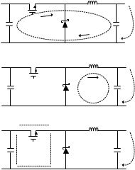 Figure 23. Current Flow in a Buck Application
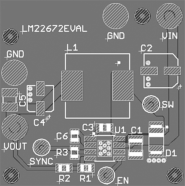
10.2 Layout Example
10.3 Thermal Considerations
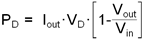
The components with the highest power dissipation are the power diode and the power MOSFET internal to the LM22672 regulator. The easiest method to determine the power dissipation within the LM22672 is to measure the total conversion losses then subtract the power losses in the diode and inductor. The total conversion loss is the difference between the input power and the output power. An approximation for the power diode loss is shown in Equation 18:
where
- VD is the diode voltage drop.
An approximation for the inductor power is shown in Equation 19:

Where:
RL is the dc resistance of the inductor.
The 1.1 factor is an approximation for the ac losses.
The regulator has an exposed thermal pad to aid power dissipation. Adding multiple vias under the device to the ground plane will greatly reduce the regulator junction temperature. Selecting a diode with an exposed pad will also aid the power dissipation of the diode. The most significant variables that affect the power dissipation of the regulator are output current, input voltage and operating frequency. The power dissipated while operating near the maximum output current and maximum input voltage can be appreciable. The junction-to-ambient thermal resistance of the LM22672 will vary with the application. The most significant variables are the area of copper in the PC board, the number of vias under the IC exposed pad and the amount of forced air cooling provided. A large continuous ground plane on the top or bottom PCB layer will provide the most effective heat dissipation. The integrity of the solder connection from the IC exposed pad to the PC board is critical. Excessive voids will greatly diminish the thermal dissipation capacity. The junction-to-ambient thermal resistance of the LM22672 SO PowerPAD package is specified in the Electrical Characteristics table. See AN-2020 Thermal Design By Insight, Not Hindsight (SNVA419) for more information.