SNVS617H April 2009 – November 2014 LM25011 , LM25011-Q1
PRODUCTION DATA.
- 1 Features
- 2 Applications
- 3 Description
- 4 Revision History
- 5 Pin Configuration and Functions
- 6 Specifications
- 7 Detailed Description
- 8 Application and Implementation
- 9 Power Supply Recommendations
- 10Layout
- 11Device and Documentation Support
- 12Mechanical, Packaging, and Orderable Information
Package Options
Mechanical Data (Package|Pins)
- DGQ|10
Thermal pad, mechanical data (Package|Pins)
- DGQ|10
Orderable Information
3 Description
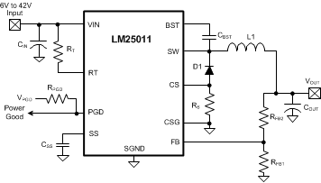
The LM25011 constant on-time step-down switching regulator features all the functions needed to implement a low-cost, efficient, buck bias regulator capable of supplying up to 2 A of load current. This high-voltage regulator contains an N-Channel Buck switch, a startup regulator, current limit detection, and internal ripple control. The constant on-time regulation principle requires no loop compensation, results in fast load transient response, and simplifies circuit implementation. The operating frequency remains constant with line and load. The adjustable valley current limit detection results in a smooth transition from constant voltage to constant current mode when current limit is reached, without the use of current limit foldback. The PGD output indicates the output voltage has increased to within 5% of the expected regulation value. Additional features include: Low output ripple, VIN under-voltage lock-out, adjustable soft-start timing, thermal shutdown, gate drive pre-charge, gate drive under-voltage lock-out, and maximum duty cycle limit.
The LM25011A has a shorter minimum off-time than the LM25011, which allows for higher frequency operation at low input voltages.
Device Information(1)
| PART NUMBER | PACKAGE | BODY SIZE (NOM) |
|---|---|---|
| LM25011 / -Q1 | HVSSOP (10) | 3.00 mm × 3.00 mm |
| LM25011A / -Q1 |
- For all available packages, see the orderable addendum at the end of the data sheet.
Typical Application
