SNVS617H April 2009 – November 2014 LM25011 , LM25011-Q1
PRODUCTION DATA.
- 1 Features
- 2 Applications
- 3 Description
- 4 Revision History
- 5 Pin Configuration and Functions
- 6 Specifications
- 7 Detailed Description
- 8 Application and Implementation
- 9 Power Supply Recommendations
- 10Layout
- 11Device and Documentation Support
- 12Mechanical, Packaging, and Orderable Information
Package Options
Mechanical Data (Package|Pins)
- DGQ|10
Thermal pad, mechanical data (Package|Pins)
- DGQ|10
Orderable Information
7.3.6 Soft-Start
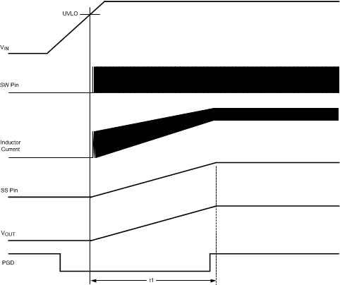
The soft-start feature allows the converter to gradually reach a steady-state operating point, thereby reducing startup stresses and current surges. Upon turn-on, when VIN reaches its undervoltage lock-out threshold an internal 10-µA current source charges the external capacitor at the SS pin to 2.51 V (t1 in Figure 17). The ramping voltage at SS ramps the non-inverting input of the regulation comparator and the output voltage, in a controlled manner. For proper operation, the soft-start capacitor should be no smaller than 1000 pF.
The LM25011 can be employed as a tracking regulator by applying the controlling voltage to the SS pin. The output voltage of the regulator tracks the applied voltage, gained up by the ratio of the feedback resistors. The applied voltage at the SS pin must be within the range of 0.5 V to 2.6 V. The absolute maximum rating for the SS pin is 3.0 V. If the tracking function causes the voltage at the FB pin to go below the thresholds for the PGD pin, the PGD pin will switch low (see the Power Good Output (PGD) section). An internal switch grounds the SS pin if the input voltage at VIN is below its undervoltage lock-out threshold or if the thermal shutdown activates. If the tracking function (described above) is used, the tracking voltage applied to the SS pin must be current limited to a maximum of 1 mA.
 Figure 17. Startup Sequence