SNVS952F December 2012 – May 2021 LM25019
PRODUCTION DATA
- 1 Features
- 2 Applications
- 3 Description
- 4 Revision History
- 5 Pin Configuration and Functions
- 6 Specifications
-
7 Detailed Description
- 7.1 Overview
- 7.2 Functional Block Diagram
- 7.3
Feature Description
- 7.3.1 Control Overview
- 7.3.2 VCC Regulator
- 7.3.3 Regulation Comparator
- 7.3.4 Overvoltage Comparator
- 7.3.5 On-Time Generator
- 7.3.6 Current Limit
- 7.3.7 N-Channel Buck Switch and Driver
- 7.3.8 Synchronous Rectifier
- 7.3.9 Undervoltage Detector
- 7.3.10 Thermal Protection
- 7.3.11 Ripple Configuration
- 7.3.12 Soft Start
- 7.4 Device Functional Modes
- 8 Application and Implementation
- 9 Power Supply Recommendations
- 10Layout
- 11Device and Documentation Support
- 12Mechanical, Packaging, and Orderable Information
Package Options
Mechanical Data (Package|Pins)
Thermal pad, mechanical data (Package|Pins)
Orderable Information
7.3.9 Undervoltage Detector
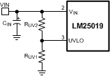
The LM25019 device contains a dual-level UVLO circuit. A summary of threshold voltages and operational states is provided in the Section 7.4. When the UVLO pin voltage is below 0.66 V, the controller is in a low-current shutdown mode. When the UVLO pin voltage is greater than 0.66 V but less than 1.225 V, the controller is in standby mode. In standby mode, the VCC bias regulator is active while the regulator output is disabled. When the VCC pin exceeds the VCC undervoltage threshold and the UVLO pin voltage is greater than 1.225 V, normal operation begins. An external set-point voltage divider from VIN to GND can be used to set the minimum operating voltage of the regulator.
UVLO hysteresis is accomplished with an internal 20-μA current source that is switched on or off into the impedance of the set-point divider. When the UVLO threshold is exceeded, the current source is activated to quickly raise the voltage at the UVLO pin. The hysteresis is equal to the value of this current times the resistance RUV2.
If the UVLO pin is wired directly to the VIN pin, the regulator begins operation once the VCC undervoltage is satisfied.
 Figure 7-3 UVLO Resistor Setting