SNVS572E July 2008 – January 2016 LM25037 , LM25037-Q1
PRODUCTION DATA.
- 1 Features
- 2 Applications
- 3 Description
- 4 Revision History
- 5 Pin Configuration and Functions
- 6 Specifications
- 7 Detailed Description
- 8 Application and Implementation
- 9 Power Supply Recommendations
- 10Layout
- 11Device and Documentation Support
- 12Mechanical, Packaging, and Orderable Information
Package Options
Mechanical Data (Package|Pins)
- PW|16
Thermal pad, mechanical data (Package|Pins)
Orderable Information
8 Application and Implementation
NOTE
Information in the following applications sections is not part of the TI component specification, and TI does not warrant its accuracy or completeness. TI’s customers are responsible for determining suitability of components for their purposes. Customers should validate and test their design implementation to confirm system functionality.
8.1 Application Information
8.1.1 Topology and Control Algorithm Choice
The LM25037 has all the features required to implement double-ended power converter topologies such as push-pull, half-bridge and full-bridge with minimum external components. One key feature is the flexibility in control algorithm selection; that is, the LM25037 can be used to implement either voltage mode control or current mode control. Designers familiar with these topologies recognize that conventionally, current mode control is used for push-pull and full-bridge topologies while voltage mode control is required for the half-bridge topology. In limited applications, voltage mode control can be used for push-pull and full-bridge topologies as well, with special care to maintain flux balance, such as using a DC-blocking capacitor in the primary (full-bridge). The goal of this section is to illustrate implementation of both current mode control and voltage mode control using the LM25037 and aid the designer in the design process.
8.1.2 Voltage Mode Control Using the LM25037
An external resistor (RFF) and capacitor (CFF) connected to VIN, AGND, and the RAMP pins is required to create a saw-tooth modulation ramp signal shown in Figure 18. The slope of the signal at RAMP will vary in proportion to the input line voltage. The varying slope provides line feed-forward information necessary to improve line transient response with voltage mode control. With a constant error signal, the on-time (tON) varies inversely with the input voltage (VIN) to stabilize the volt-second product of the transformer primary. Using a line feed-forward ramp for PWM control requires very little change in the voltage regulation loop to compensate for changes in input voltage, as compared to a fixed slope oscillator ramp. Furthermore, voltage mode control is less susceptible to noise and does not require leading edge filtering, and is therefore a good choice for wide input range power converters. Voltage mode control requires a more complicated compensation network, due to the complex-conjugate poles of the L-C output filter.
In push-pull and full-bridge topologies, any asymmetry in the volt-second product applied to primary in one phase may not be cancelled by subsequent phase, possibly resulting in a DC current build-up in the transformer, which pushes the transformer core towards saturation. Special care in the transformer design, such as gapping the core, or adding ballasting resistance in the primary is required to rectify this imbalance when using voltage mode control with these topologies. Current mode control naturally corrects for any volt-second asymmetry in the primary.
The recommended capacitor value range for CFF is from 100 pF to 1500 pF. Referring to Figure 18, it can be seen that value CFF must be small enough such that the capacitor can be discharged within the clock (CLK) pulse width each cycle. The CLK pulse width is same as the dead-time set by RT2. The minimum possible dead-time for LM25037 is 50 ns and the internal discharge FET RDS(ON) is 5 Ω (typical),
The value of RFF required can be calculated using Equation 3.

For example, assuming a VRamp of 1 volt at VINmin (a good compromise of signal range and noise immunity), oscillator frequency, FOSC of 250 kHz, VINmin of 24 V, and CFF = 270 pF results in a value for RFF of 348 kΩ.
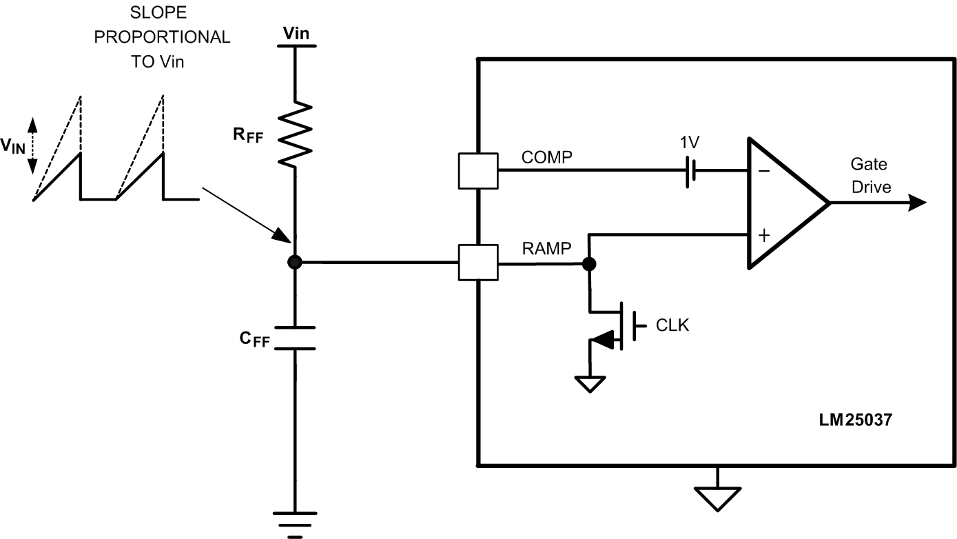 Figure 18. Feed-Forward Voltage Mode Configuration
8.1.3 Current Mode Control Using the LM25037
The LM25037 can be configured in current mode control by applying the primary current signal into the RAMP pin. One way to achieve this is shown in Figure 19, which depicts a simplified push-pull converter. The primary current is sensed using a sense resistor and the current information is then filtered and applied to the RAMP pin through capacitor Cslope, for use as the modulation ramp. It can be seen that the signal applied to the RAMP pin consists of the primary current information from the CS pin plus an additional ramp for slope compensation, added by Rslope and Cslope.
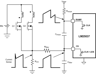 Figure 19. Current Mode Configuration
Current mode control inherently provides line voltage feed-forward, cycle-by-cycle current limiting and ease of loop compensation as it removes the additional pole due to output inductor. Also, in push-pull and full-bridge converters, current mode control inherently balances volt-second product in both the phases by varying the duty cycle as needed to terminate the cycle at the same peak current for each output phase. For duty cycles greater than 50% (25% for each phase), peak current mode controlled circuits are subject to sub-harmonic oscillation. Sub-harmonic oscillation is normally characterized by observing alternating wide and narrow duty cycles at the controller output. Adding an artificial ramp (slope compensation) to the current sense signal will eliminate this potential oscillation. Current mode control is also susceptible to noise and layout considerations. TI recommends placing the CFilter and Cslope as close to the IC as possible to avoid any noise pickup and trace inductance. When the converter is operating at low duty cycles and light load, the primary current amplitude is small and is susceptible to noise. The artificial ramp, added to avoid sub-harmonic oscillations, provides additional benefits by improving the noise immunity of the converter.
Configuration and component selection for current mode control is recommended as follows: The current sense resistor is selected such that during overcurrent condition, the voltage across the current sense resistor is above the minimum CS threshold of 220 mV. TI recommends setting the impedances of RFilter and CFilter as seen from Cslope at relatively low values, so that the slope compensation is primarily dictated by Rslope and Cslope components. For example, if the filtering time (RFilter and CFilter) for leading edge noise is selected for 50 ns and if the value selected for RFilter = 25 Ω, then

Resulting in a value of CFilter = 680 pF (approximated to a standard value). In general, the amount of slope compensation required to avoid sub-harmonic oscillation is equal to at least one-half the down-slope of the output inductor current, transformed to the primary. To mitigate subharmonic oscillation after one switching period, the slope compensation must be equal to one times the down slope of the filter inductor current transformed to primary. This is known as deadbeat control. For circuits where primary current is sensed, the amount of slope compensation for dead-beat control can be calculated using Equation 5.

where
- Turns-Ratio is referred with respect to the primary.
For example, for a 5-V output converter with a turns ratio between secondary and primary of 1:2, an oscillator frequency (FOSC) of 250 kHz, a filter inductance of 4 µH (LFilter) and a current sense resistor (RCS) of 32 mΩ, slope compensation of 80 mV will suffice. The slope compensation volts that results from Equation 5 is the maximum voltage of the artificial ramp added linearly to the RAMP pin till the end of maximum switching period. For circuits where a current sense tramsformer is used for primary current sensing, the turns-ratio of the current sense transformer must be considered.
Cslope should be selected such that it can be fully discharged by the internal RAMP discharge FET. TI recommends capacitor values ranging from 100 pF to 1500 pF. The value must be small enough such that the capacitor can be discharged within the clock (CLK) pulse width each cycle.
Rslope can be selected using Equation 6.

For example, with a Cslope of 1500 pF, FOSC of 250 kHz, reference voltage of 5 V (VREF), slope compensation of 80 mV and Rfilter = 25 Ω results in Rslope value of 165 kΩ.
8.1.4 VIN and VCC
The voltage applied to the VIN pin, which may be the same as the system voltage applied to the power transformer’s primary (VPWR), can vary in the range from 5.5 V to 75 V. The current into the VIN pin depends primarily on the gate charge provided by the output drivers, the switching frequency, and any external loads on the VCC and REF pins. TI recommends using the filter shown in Figure 20 to suppress transients that may occur at the input supply. This is particularly important when VIN is operated close to the maximum operating rating of the LM25037.
When power is applied to VIN and the UVLO pin voltage is greater than 0.45 V, the VCC regulator is enabled and supplies current into an external capacitor connected to the VCC pin. When the voltage on the VCC pin reaches the regulation point of 7.7 V, the voltage reference (REF) is enabled. The reference regulation set point is 5 V. The outputs (OUTA and OUTB) are enabled when the two bias regulators reach their set point and the UVLO pin potential is greater than 1.25 V. In typical applications, an auxiliary transformer winding is connected through a diode to the VCC pin. This winding must raise the VCC voltage above 8.1 V to shut off the internal start-up regulator.
After the outputs are enabled and the external VCC supply voltage has begun supplying power to the IC, the current into the VIN pin drops below 1 mA. VIN should remain at a voltage equal to or greater than the VCC voltage to avoid reverse current through protection diodes.
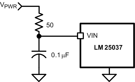 Figure 20. Input Transient Protection
8.1.5 Applications With >75-V Input
For applications where the system input voltage exceeds 75 V or the IC power dissipation is of concern, the LM25037 can be powered from an external start-up regulator as shown in Figure 21. In this configuration, the VIN and the VCC pins should be connected together. The voltage at the VCC and VIN pins must be at least 5.5 V (> Maximum VCC UV voltage) yet not exceed 14 V. An auxiliary winding can be used to reduce the power dissipation in the external regulator once the power converter is active. The NPN base-emitter reverses breakdown voltage, which can be as low as 5 V for some transistors, should be considered when selecting the transistor.
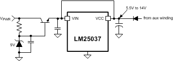 Figure 21. Start-Up Regulator for VPWR >75 V
8.1.6 Current Sense
The CS pin should receive an input signal representative of the transformer’s primary current, either from a current sense transformer or from a resistor in series with the source of the OUTA and OUTB MOSFET switches. In both cases, the sensed current creates a voltage ramp across R1, and the RF/CF filter suppresses noise and transients as shown in Figure 22 and Figure 23. R1, RF and CF should be placed as close to the LM25037 as possible, and the ground connection from the current sense transformer, or R1, should be a dedicated track to the AGND pin. The current sense components must provide greater than 220 mV at the CS pin when an overcurrent condition exists.
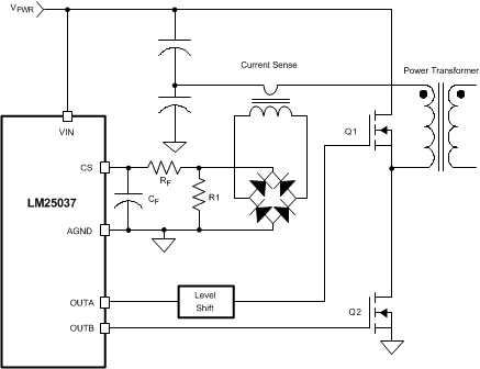 Figure 22. Current Sense Using Transformer
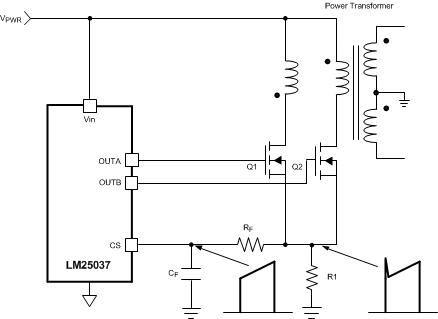 Figure 23. Current Sense Using Current Sense Resistor (R1)
8.1.7 UVLO Divider Selection
A dedicated comparator connected to the UVLO pin detects an input undervoltage condition. When the UVLO pin voltage is less than 0.45 V, the LM25037 controller is in a low current shutdown mode. For a UVLO pin voltage greater than 0.45 V but less than 1.25 V, the controller is in standby mode with VCC and REF regulators active but no switching. Once the UVLO pin voltage is greater than 1.25 V, the controller is fully enabled. When the UVLO pin voltage rises above the 1.25-V threshold, an internal 22-µA current source as shown in Figure 24, is activated thus providing threshold hysteresis. The 22-µA current source is deactivated when the voltage at the UVLO pin falls below 1.25 V. Resistance values for R1 and R2 can be determined using Equation 7.
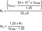
where
- VPWR is the desired turnon voltage and VHYS is the desired UVLO hysteresis at VPWR.
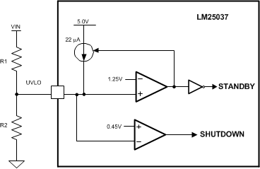 Figure 24. Basic UVLO Configuration
For example, if the LM25037 is to be enabled when VPWR reaches 33 V, and disabled when VPWR decreases to 30 V, R1 should be 113 kΩ, and R2 should be 4.42 kΩ. The voltage at the UVLO pin should not exceed 7 V at any time. Be sure to check both the power and voltage rating (0603 resistors can be rated as low as 50 V) for the selected R1 resistor. To maintain the UVLO threshold accuracy, TI recommends a resistor tolerance of 1% or better.
Remote control of the LM25037 operational modes can be accomplished with open-drain device(s) connected to the UVLO pin as shown in Figure 25.
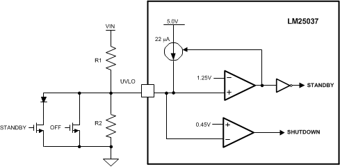 Figure 25. Remote Standby and Disable Control
8.1.8 Hiccup Mode Current Limit Restart (RES)
The basic operation of the hiccup mode current limit is described in the functional description. The delay time to the initiation of a hiccup cycle is programmed by the selection of the RES pin capacitor CRES as illustrated in Figure 26.
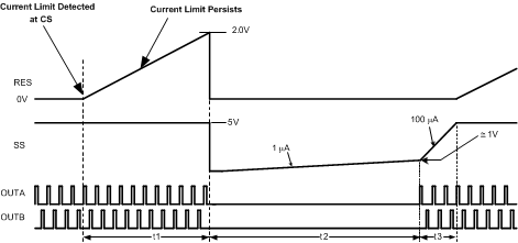 Figure 26. Hiccup Over-Load Restart Timing
In the case of continuous cycle-by-cycle current limit detection at the CS pin, the time required for CRES to reach the 2-V hiccup mode threshold is given by Equation 8:

For example, if CRES = 0.01 µF the time t1 is approximately 2 ms. The cool down time, t2 is set by the soft-start capacitor (CSS) and the internal 1 µA SS current source, and is equal to Equation 9:

If CSS = 0.01 µF, t2 is ≊10 ms.
The soft-start time t3 is set by the internal 100-µA current source, and is equal to Equation 10:

If CSS = 0.01 µF, t3 is ≊ 400 µs.
The time t2 provides a periodic cool-down time for the power converter in the event of a sustained overload or short circuit. This off time results in lower average input current and lower power dissipation within the power components. TI recommends that the ratio of t2 / (t1 + t3) be in the range of 5 to 10 to take advantage of this feature.
If the application requires no delay from the first detection of a current limit condition to the onset of the hiccup mode (t1 = 0), the RES pin can be left open (no external capacitor). If it is desired to disable the hiccup mode entirely, the RES pin should be connected to ground (AGND).
8.2 Typical Application
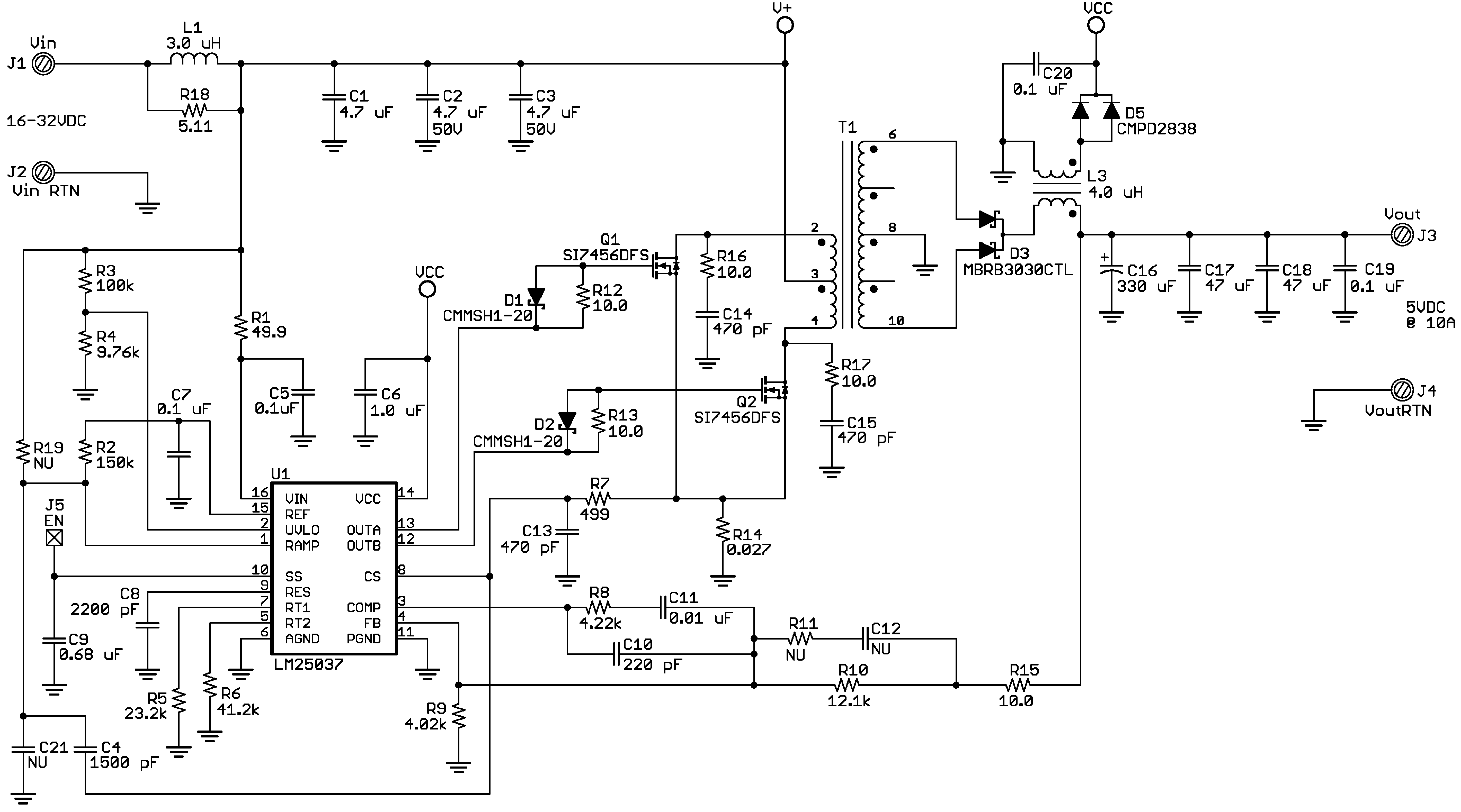
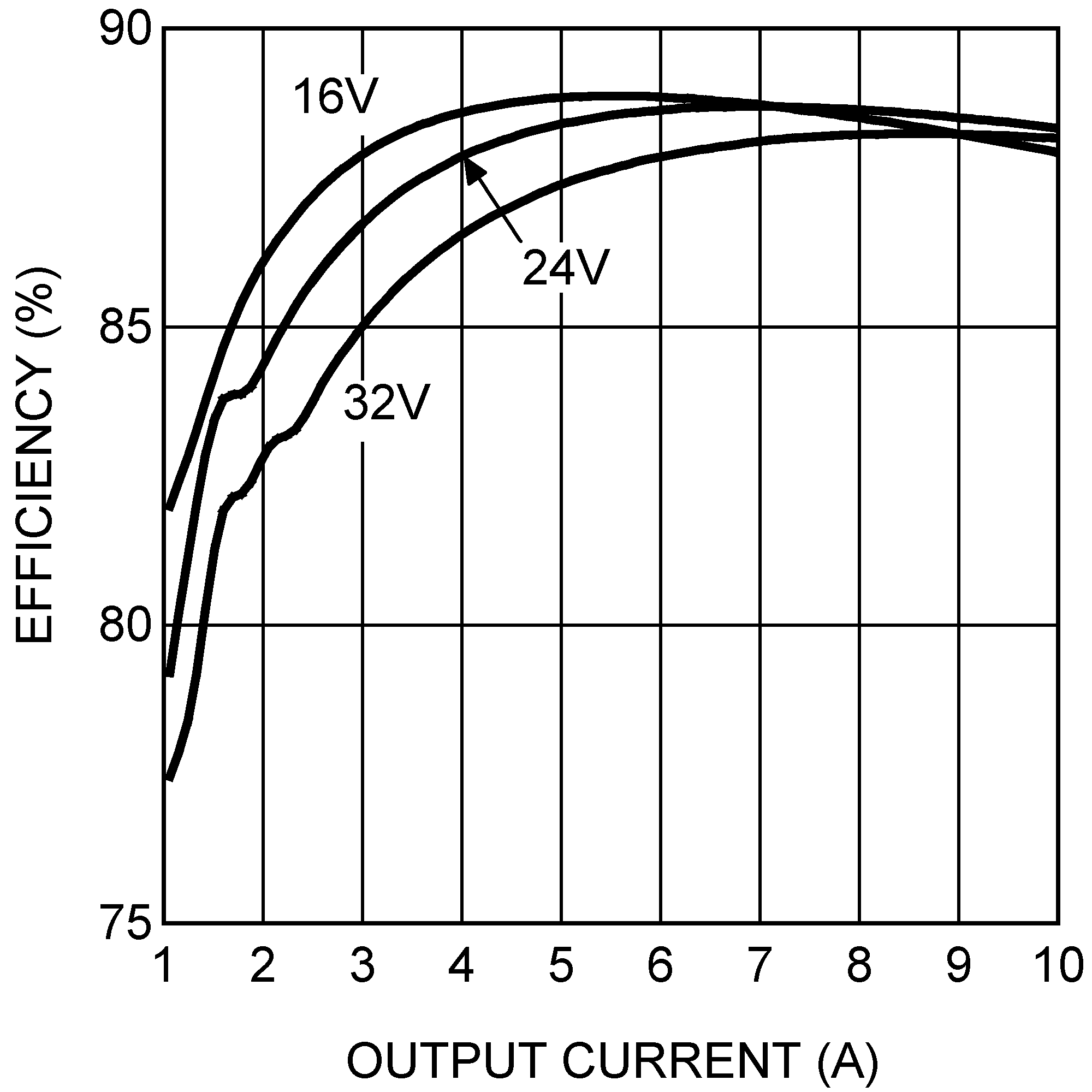
Figure 27 shows an example of an LM25037-controlled 50-W push-pull converter. The converter provides a single regulated 5-V output at 10 A, from an input voltage range of 16 V to 32 V. The converter is configured for current-mode control with external slope compensation. An auxiliary winding on the output filter inductor is used to supply the VCC voltage externally – the VCC level is chosen higher than the internal regulator level, to reduce the power dissipation in the LM25037 IC.
8.2.1 Design Requirements
The LM25037 evaluation board is designed to provide the design engineer with a fully functional power converter based on push-pull topology to evaluate the LM25037 controller. Table 1 lists the performance of the evaluation board.
Table 1. Design Parameters
| DESIGN PARAMETER | VALUE |
|---|---|
| Input Voltage Range, VIN | 16 V to 32 V |
| UVLO On/Off Levels | 14 V On (rising)/11 V Off (falling) |
| Output Voltage VOUT | 5 V |
| Output Current IOUT | 10 A |
| Oscillator frequency (2x Fsw per phase) | 250 kHz |
| Switching frequency Fsw (per phase) | 125 kHz |
8.2.2 Detailed Design Procedure
8.2.2.1 Oscillator Frequency and Maximum Duty Cycle
The LM25037 oscillator frequency will be twice the switching frequency of each switch in the push-pull power stage, that is, Fosc = 2 × Fsw.
First of all the dead-time resistor value RT2 is calculated. The recommended range of dead-time is 50 ns to 250 ns. A value of 200 ns is chosen, which will set a maximum duty cycle of approximately 95%. From Equation 11, the required value of resistor on the RT2 pin (R6 in Figure 27) is calculated using Equation 11.

The E96 value of 41.2 kΩ is used.
Next, knowing the resistor value on RT2 pin, the required resistor value for the RT1 pin (R5 in Figure 27) can be calculated from Equation 12.

8.2.2.2 Power Stage Design
Referring to the schematic in Figure 27, the push-pull power stage primarily consists of input capacitors C1, C2, and C3, power MOSFETs Q1 and Q2, power transformer T1, output rectifier D3, and output filter L3 and C16, C17, C18. The push-pull transformer has two out-of-phase primary windings, centre-tapped, and two out-of-phase secondary windings, also centre-tapped.
The centre-tap of the primary is connected to the DC input voltage, VIN. The other end of each primary winding connects to Q1 and Q2 respectively. The push-pull controller alternately drives Q1 and Q2 180° out of phase, so that the voltage across each winding is approximately equal to Vin when its respective switch (Q1 or Q2) is turned on.
On the secondary side, the voltage across each secondary winding will be the same as Vin, scaled by the transformer turns ratio Ns/Np. Double-diode D3 alternately rectifies the positive voltage across each secondary winding, to generate a full-wave rectified positive-voltage pulse-train at D3 cathode. This pulse train is then filtered to DC by output filter L3 and C16/C17/C18.
The LM25037 modulates the duty cycle of the pulses to regulate the output voltage to the required level. The duty cycle is adjusted with input line voltage to regulate VOUT:

Choosing a transformer with turns ratio Np/Ns = 2, maximum duty cycle will occur at minimum operating VIN, which will be approximately 11 V (UVLO turnoff point):

Thus there is sufficient margin to the oscillator 95% Dmax setting (set by choice of RT2 resistor).
Knowing the duty cycle (D), Fosc frequency and turns ratio, the output inductor (LOUT) peak-to-peak ripple current in Continuous Conduction Mode (CCM) can be estimated. At minimum VIN of 16 V:

And at a maximum VIN of 32 V:

8.2.2.3 UVLO Setting
To ensure start-up at the required minimum system input voltage of 14 V, with the 3 V of hysteresis to the desired turnoff level, the UVLO divider resistors R3 and R4 are calculated as follows using Equation 17:

This is rounded down to a convenient value of 100 kΩ. This reduces the effective hysteresis to approximately 2.5 V.
To set the turnon level to 14 V, calculate the lower UVLO divider resistor:

The nearest E96 value of 9.76 kΩ is used.
8.2.2.4 VIN, VCC, Start-Up
To reduce the power dissipation in the internal start-up regulator on the VIN pin, a separate external VCC supply is used. This is derived from the auxiliary winding on the output filter inductor L3. The auxiliary to main inductor winding turns ratio is 2:1, so when VOUT is regulated at 5 V, the auxiliary VCC will be approximately 10 V. This is sufficiently greater than the maximum internal VCC regulator level of 8 V to back-bias the internal regulator after start-up.
8.2.2.5 Current Sense Resistor
The CS pin is used to implement cycle-by-cycle current limit, if the peak current exceeds the internal threshold – 255 mV typical, 220 mV minimum. This limit is used to choose the value of the current-sense resistor R14.
Knowing the maximum output inductor peak-peak ripple current in CCM, and the turns ratio the transformer (Ns/Np), the current-limit point can be set as required. Given that the full load output current is 10 A, the current limit target is set at 150%, or 15 A. Thus the required value for R14 may be calculated – it must generate a voltage at the CS pin no higher than the internal cycle-by-cycle limit of minimally 0.22 V at the current limit level at the output.

The nearest E96 value of 27 mΩ is chosen for R14. A small filter R7, C13 can be optionally added to filter the leading-edge current spike in the current-sense waveform, if the internal 65-ns leading-edge blanking time is not sufficient. In this case, a 499-Ω resistor and 470-pF capacitor are used, for approximately 235-ns filter time constant.
8.2.2.6 Current-Mode Control
Push-pull power stages always use peak current-mode control rather than voltage-mode, to keep the transformer balanced, and avoid stair-case saturation. Ideally, the push-pull transformer flux should return to zero at the end of each switching cycle. However, due to small imbalances between each phase of the primary (for example, slightly different Rdson between primary FETs Q1 and Q2), the peak current can be slightly different in each phase. This causes the transformer flux to become slightly biased away from zero after a complete switching. After several switching cycles, this small net imbalance per cycle can accumulate or stair-case to the point that the transformer starts to saturate in one or other direction.
By using current-mode control and connecting the sources of both FETs Q1 and Q2 to the same current sense resistor R14, the LM25037 controller ensures that the same exact peak current flows in each phase of the primary. This means that the transformer has identical peak flux swing in each direction, so it always returns to zero at the end of each switching cycle.
The CS pin ramp is capacitively-coupled to the RAMP pin (input to the internal PWM comparator) using C4, where it is then also summed with the slope compensation ramp (see Slope Compensation Ramp).
8.2.2.7 Slope Compensation Ramp
Because current-mode control is being used, slope compensation is required to prevent instability and sub-harmonic oscillation at power stage duty cycles above 50%. For the push-pull topology, this means slope compensation is required when the switch duty cycle is above 25% of the overall switching period. For stability, the slope compensation ramp should be at least half the output inductor current downslope, or more ideally equal to it.
The output inductor downslope, scaled by the transformer turns ratio and current-sense resistor R14, can be expressed as:

Resistor R2 and capacitor C4 are used to generate the slope compensation ramp and sum it with the current-sense signal at the CS pin. The RC time constant should be quite large compared to the oscillator period to make the ramp reasonably linear. Assuming that RC >> Tosc, the slope of the ramp is approximately:

Choosing C4 = 1.5 nF, the value of R2 can be calculated using Equation 22 to achieve the required slope.

A lower value of 150 kΩ is chosen for R2 to allow for tolerances and to ensure a sufficient slope compensation ramp under all conditions.
8.2.2.8 Soft-start
The soft-start delay to commencement of first PWM switching can be calculated using Equation 23.

Thereafter, the soft-start ramp time depends on the power stage design and the operating conditions (input voltage and output load).
8.2.2.9 Overload Timer
With a timing capacitor C8 of 2.2 nF on the RES pin, the hiccup-mode timing and duty cycle can be calculated for a sustained overcurrent condition.
Hiccup-mode current-limit persist time t1:

Hiccup-mode cool-down off-time t2:

Thus the hiccup-mode duty cycle is approximately:

8.2.2.10 Output Voltage Feedback
In this example, the output of the DC-DC converter is non-isolated from the input, so resistor divider R15, R10, R9 are used to scale VOUT down to the required 1.25-V reference level at the FB pin.
Because current-mode control removes the pole due to the output inductor, the loop compensation components R8, C10, C11 are chosen to implement a simpler Type II compensator. For further details about control loop design and Type II compensator design, see application notes Seminar 300 Topic 2 - Apdx A - Error Amplifier and Compensation Network Design (SLUP069) or Seminar 1400 Topic 5 Designing Stable Control Loops (SLUP173).
8.2.3 Application Curves
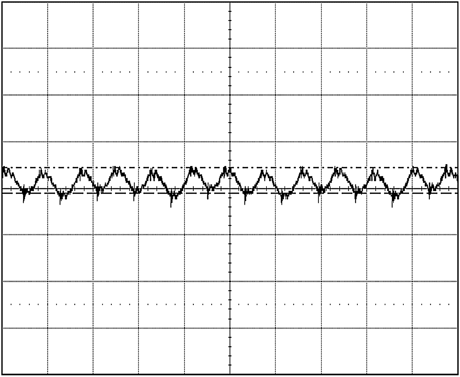
| Conditions: | |
| Input Voltage = 24 VDC | Output Current = 10 A |
| Bandwidth Limit = 20 MHz | |
| Trace: | |
| Output Ripple, V/div = 50 mV | Horizontal Resolution = 5 µs/div |
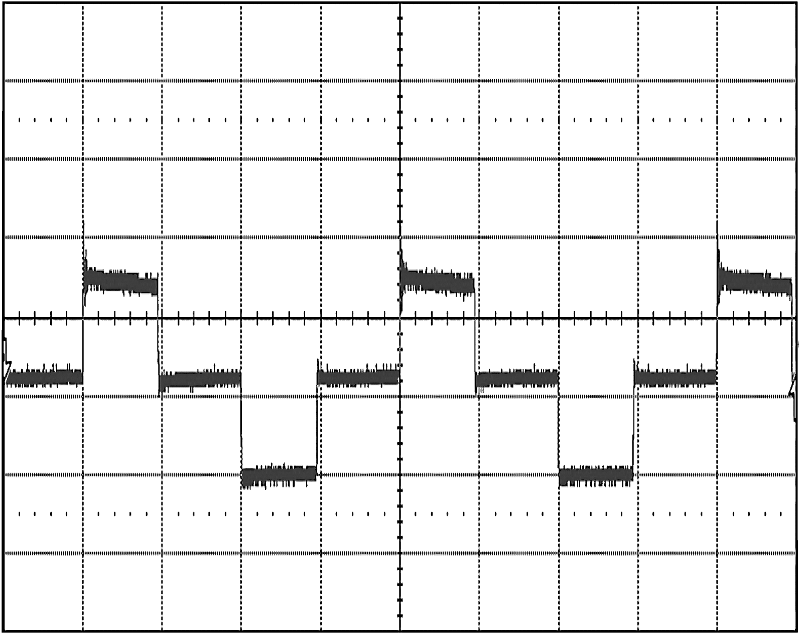
| Conditions: | |
| Input Voltage = 24 VDC | Output Current = 5 A |
| Trace: | |
| Q1 drain-to-source voltage, V/div = 20 V | Horizontal Resolution = 2 µs/div |
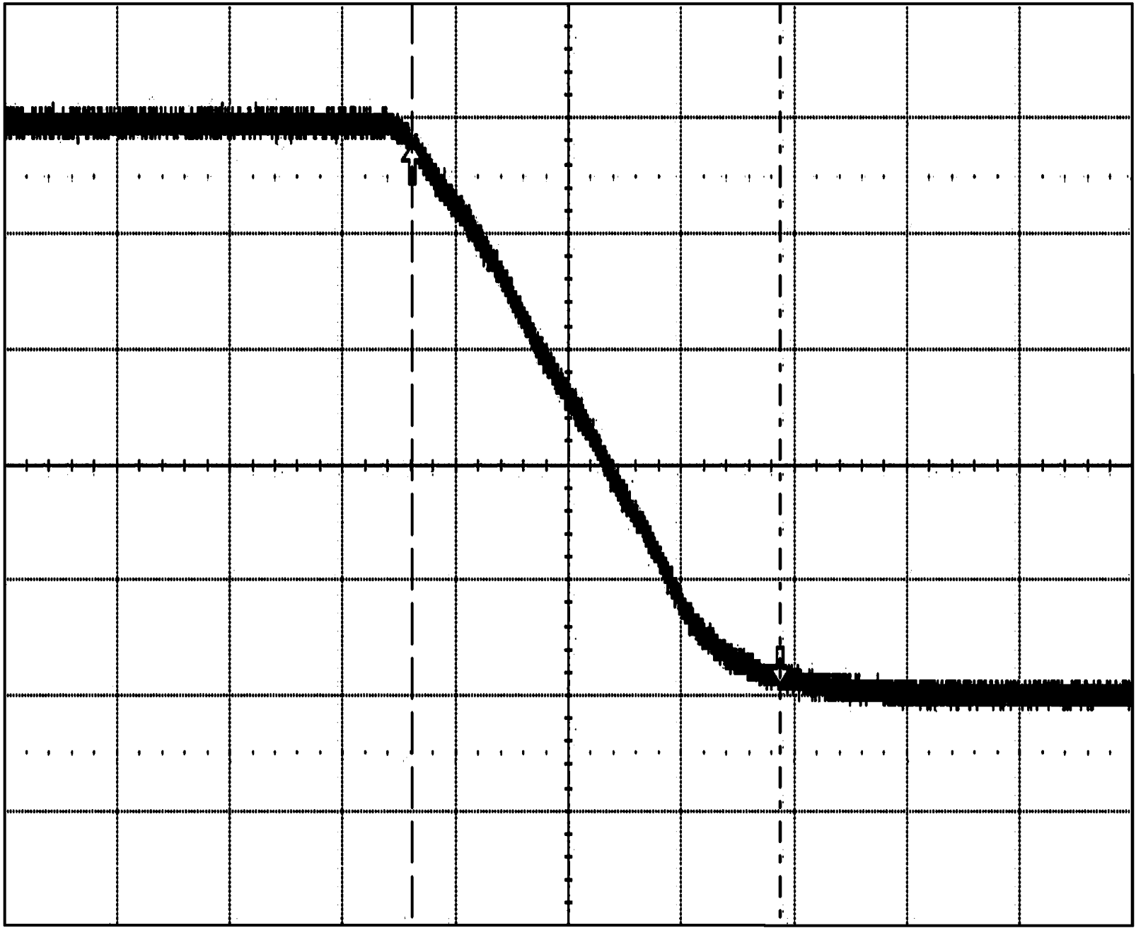
| Conditions: Input Voltage = 24 VDC | |||
| Trace: Output Voltage, V/div = 1 V | |||
| Horizontal Resolution = 0.5 ms/div | |||
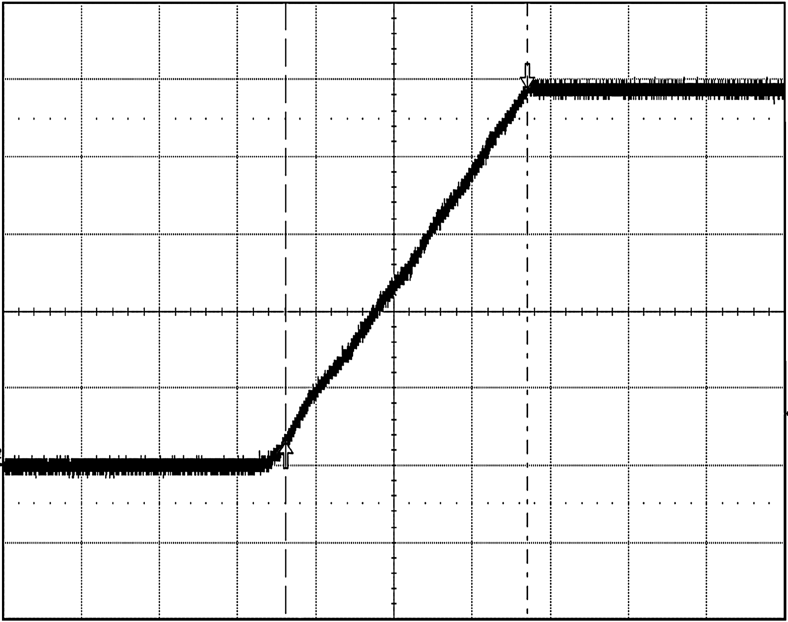
| Conditions: | |
| Input Voltage = 24 VDC | Output Current = 10 A |
| Trace: | |
| Output Voltage, V/div = 1 V | Horizontal Resolution = 0.5 ms/div |
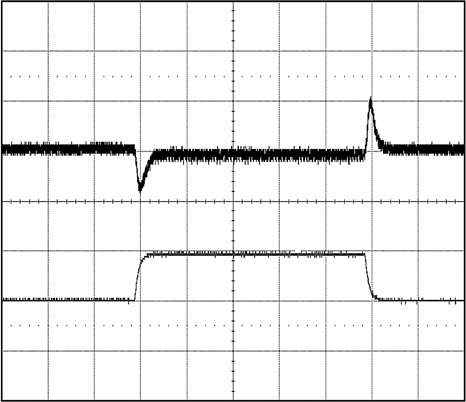
| Conditions: | ||
| Input Voltage = 24 VDC | Output Current = 5 to 10 A | |
| Bandwidth Limit = 20 MHz | ||
| Traces: | ||
| Bottom Trace: Output current | A/div = 5 A | |
| Top Trace: Output voltage response | V/div = 100 mV | |
| Horizontal Resolution = 200 µs/div | ||
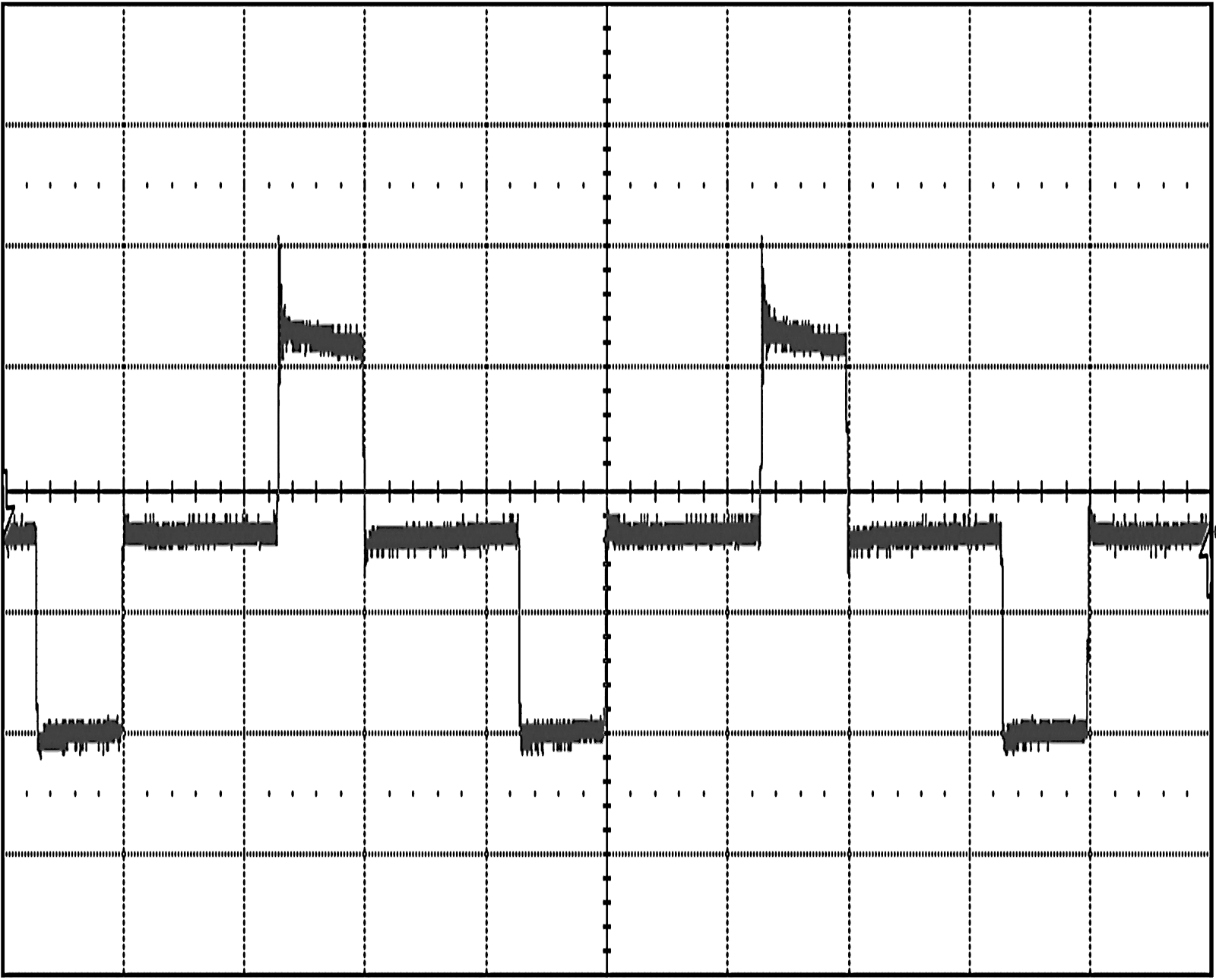
| Conditions: | |
| Input Voltage = 32 VDC | Output Current = 5 A |
| Trace: | |
| Q1 drain to source voltage, V/div = 20 V | Horizontal Resolution = 2 µs/div |
