-
LM25183-Q1 42-VIN PSR Flyback DC/DC Converter with 65-V, 2.5-A MOSFET
- 1 Features
- 2 Applications
- 3 Description
- 4 Revision History
- 5 Pin Configuration and Functions
- 6 Specifications
-
7 Detailed Description
- 7.1 Overview
- 7.2 Functional Block Diagram
- 7.3
Feature Description
- 7.3.1 Integrated Power MOSFET
- 7.3.2 PSR Flyback Modes of Operation
- 7.3.3 Setting the Output Voltage
- 7.3.4 Control Loop Error Amplifier
- 7.3.5 Precision Enable
- 7.3.6 Configurable Soft Start
- 7.3.7 External Bias Supply
- 7.3.8 Minimum On-Time and Off-Time
- 7.3.9 Overcurrent Protection
- 7.3.10 Thermal Shutdown
- 7.4 Device Functional Modes
-
8 Application and Implementation
- 8.1 Application Information
- 8.2
Typical Applications
- 8.2.1
Design 1: Wide VIN, Low IQ PSR Flyback Converter Rated at 12 V, 0.6 A
- 8.2.1.1 Design Requirements
- 8.2.1.2
Detailed Design Procedure
- 8.2.1.2.1 Custom Design With WEBENCH® Tools
- 8.2.1.2.2 Custom Design With Excel Quickstart Tool
- 8.2.1.2.3 Flyback Transformer – T1
- 8.2.1.2.4 Flyback Diode – DFLY
- 8.2.1.2.5 Leakgae Inductance Clamp Circuit – DF, DCLAMP
- 8.2.1.2.6 Output Capacitor – COUT
- 8.2.1.2.7 Input Capacitor – CIN
- 8.2.1.2.8 Feedback Resistor – RFB
- 8.2.1.2.9 Thermal Compensation Resistor – RTC
- 8.2.1.2.10 UVLO Resistors – RUV1, RUV2
- 8.2.1.2.11 Soft-Start Capacitor – CSS
- 50
- 8.2.2 Application Curves
- 8.2.3 Design 2: PSR Flyback Converter With Dual Outputs of 15 V and –15 V at 0.3 A
- 8.2.1
Design 1: Wide VIN, Low IQ PSR Flyback Converter Rated at 12 V, 0.6 A
- 9 Power Supply Recommendations
- 10Layout
- 11Device and Documentation Support
- 12Mechanical, Packaging, and Orderable Information
- IMPORTANT NOTICE
Package Options
Mechanical Data (Package|Pins)
- NGU|8
Thermal pad, mechanical data (Package|Pins)
Orderable Information
LM25183-Q1 42-VIN PSR Flyback DC/DC Converter with 65-V, 2.5-A MOSFET
1 Features
- AEC-Q100-qualified for automotive
applications
- Device temperature grade 1: –40°C to 125°C ambient temperature range
- Functional Safety-Capable
- Designed for reliable and rugged
applications
- Wide input voltage range of 4.5 V to 42 V
- Robust solution with only one component crossing the isolation barrier
- ±1.5% total output regulation accuracy
- Optional VOUT temperature compensation
- –40°C to +150°C junction temperature range
- Integration reduces solution size
and cost
- Integrated 65-V, 0.11-Ω power MOSFET
- No optocoupler or transformer auxiliary winding required for VOUT regulation
- High-efficiency PSR flyback
operation
- Quasi-resonant MOSFET turnoff in BCM
- Single- and multi-output implementations
- Ultra-low conducted and radiated
EMI signatures
- Soft switching avoids diode reverse recovery
- Optimized for CISPR 25 Class 5 requirement
- Create a custom flyback regulator design using WEBENCH® Power Designer
2 Applications
- Automotive HEV/EV powertrain systems
- Sub-AM band automotive body electronics
- Traction inverter: IGBT and SiC driver supplies
3 Description
The LM25183-Q1 is a primary-side regulated (PSR) flyback converter with high efficiency over a wide input voltage range of 4.5 V to 42 V. The isolated output voltage is sampled from the primary-side flyback voltage. The high level of integration results in a simple, reliable, and high-density design with only one component crossing the isolation barrier. Boundary conduction mode (BCM) switching enables a compact magnetic solution and better than ±1.5% load and line regulation performance. An integrated 65-V power MOSFET provides output power up to 10 W with enhanced headroom for line transients.
The LM25183-Q1 simplifies the implementation of isolated DC/DC supplies with optional features to optimize performance for the target end equipment. The output voltage is set by one resistor, while an optional resistor improves output voltage accuracy by negating the thermal coefficient of the flyback diode voltage drop. Additional features include an internally-fixed or externally-programmable soft-start, precision enable input with hysteresis for adjustable line UVLO, hiccup-mode overload protection, and thermal shutdown protection with automatic recovery.
The LM25183-Q1 converter is qualified to automotive AEC-Q100 grade 1 and is available in 8-pin WSON package with 0.8-mm pin pitch and wettable flanks.
| PART NUMBER | PACKAGE(1) | BODY SIZE (NOM) |
|---|---|---|
| LM25183-Q1 | WSON (8) | 4.00 mm × 4.00 mm |
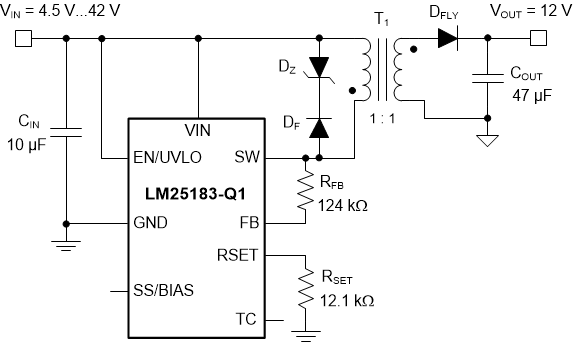
 Typical Application
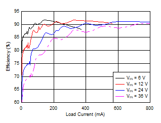
 Typical Efficiency, VOUT = 12
V
Typical Efficiency, VOUT = 12
V5 Pin Configuration and Functions
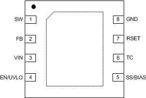
 Figure 5-1 8-Pin WSON NGU Package With Wettable Flanks
(Top View)
Figure 5-1 8-Pin WSON NGU Package With Wettable Flanks
(Top View)Pin Functions
| PIN | I/O(1) | DESCRIPTION | |
|---|---|---|---|
| NO. | NAME | ||
| 1 | SW | P | Switch node that is internally connected to the drain of the N-channel power MOSFET. Connect to the primary-side switching terminal of the flyback transformer. |
| 2 | FB | I | Primary-side feedback pin. Connect a resistor from FB to SW. The ratio of the FB resistor to the resistor at the RSET pin sets the output voltage. |
| 3 | VIN | P/I | Input supply connection. Source for internal bias regulators and input voltage sensing pin. Connect directly to the input supply of the converter with short, low impedance paths. |
| 4 | EN/UVLO | I | Enable input and undervoltage lockout (UVLO) programming pin. If the EN/UVLO voltage is below 1 V, the converter is in shutdown mode with all functions disabled. If the EN/UVLO voltage is greater than 1 V and below 1.5 V, the converter is in standby mode with the internal regulator operational and no switching. If the EN/UVLO voltage is above 1.5 V, the start-up sequence begins. |
| 5 | SS/BIAS | I | Soft start or bias input. Connect a capacitor from SS/BIAS to GND to adjust the output start-up time and input inrush current. If SS/BIAS is left open, the internal 6-ms soft-start timer is activated. Connect an external supply to SS/BIAS to supply bias to the internal voltage regulator and enable internal soft start. |
| 6 | TC | I | Temperature compensation pin. Tie a resistor from TC to RSET to compensate for the temperature coefficient of the forward voltage drop of the secondary diode, thus improving regulation at the secondary-side output. |
| 7 | RSET | I | Reference resistor tied to GND to set the reference current for FB. Connect a 12.1-kΩ resistor from RSET to GND. |
| 8 | GND | G | Analog and power ground. Ground connection of internal control circuits and power MOSFET. |
6 Specifications
6.1 Absolute Maximum Ratings
| MIN | MAX | UNIT | ||
|---|---|---|---|---|
| Input voltage | VIN to GND | –0.3 | 45 | V |
| EN/UVLO to GND | –0.3 | 45 | ||
| TC to GND | –0.3 | 6 | ||
| SS/BIAS to GND | –0.3 | 14 | ||
| FB to GND | –0.3 | 45.3 | ||
| FB to VIN | –0.3 | 0.3 | ||
| RSET to GND | –0.3 | 3 | ||
| Output voltage | SW to GND | –1.5 | 70 | V |
| SW to GND (20-ns transient) | –3 | |||
| Operating junction temperature, TJ | –40 | 150 | °C | |
| Storage temperature, Tstg | –55 | 150 | °C | |
6.2 ESD Ratings
| VALUE | UNIT | ||||
|---|---|---|---|---|---|
| V(ESD) | Electrostatic discharge | Human body model (HBM), per AEC Q100-002 HBM ESD Classification Level 2 (1) |
±2000 | V | |
| Charged device model (CDM), per AEC Q100-011 CDM ESD Classification Level C4B |
All pins except 1, 4, 5, and 8 | ±500 | |||
| Pins 1, 4, 5, and 8 | ±750 | ||||
6.3 Recommended Operating Conditions
| MIN | NOM | MAX | UNIT | ||
|---|---|---|---|---|---|
| VIN | Input voltage | 4.5 | 42 | V | |
| VSW | SW voltage | 65 | V | ||
| VEN/UVLO | EN/UVLO voltage | 42 | V | ||
| VSS/BIAS | SS/BIAS voltage | 13 | V | ||
| TJ | Operating junction temperature | –40 | 150 | °C | |