SNVS479H January   2007  – August 2017 LM25575

PRODUCTION DATA.  

  1. Features
  2. Applications
  3. Description
    1.     Device Images
      1.      Simplified Application Schematic
  4. Revision History
  5. Pin Configuration and Functions
    1.     Pin Functions
  6. Specifications
    1. 6.1 Absolute Maximum Ratings
    2. 6.2 ESD Ratings
    3. 6.3 Recommended Operating Conditions
    4. 6.4 Thermal Information
    5. 6.5 Electrical Characteristics
    6. 6.6 Typical Characteristics
  7. Detailed Description
    1. 7.1 Overview
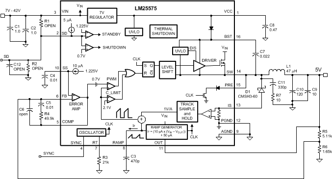
    2. 7.2 Functional Block Diagram
    3. 7.3 Feature Description
      1. 7.3.1 High Voltage Start-Up Regulator
    4. 7.4 Device Functional Modes
      1. 7.4.1 Shutdown and Stand-by Mode
      2. 7.4.2 Error Amplifier and PWM Comparator
      3. 7.4.3 Ramp Generator
      4. 7.4.4 Maximum Duty Cycle and Input Drop-out Voltage
      5. 7.4.5 Current Limit
      6. 7.4.6 Soft-Start
      7. 7.4.7 Boost Pin
      8. 7.4.8 Thermal Protection
  8. Application and Implementation
    1. 8.1 Application Information
      1. 8.1.1  External Components
      2. 8.1.2  R3 (RT)
      3. 8.1.3  L1
      4. 8.1.4  C3 (CRAMP)
      5. 8.1.5  C9, C10
      6. 8.1.6  D1
      7. 8.1.7  C1, C2
      8. 8.1.8  C8
      9. 8.1.9  C7
      10. 8.1.10 C4
      11. 8.1.11 R5, R6
      12. 8.1.12 R1, R2, C12
      13. 8.1.13 R7, C11
      14. 8.1.14 R4, C5, C6
      15. 8.1.15 BIas Power Dissipation Reduction
    2. 8.2 Typical Application
      1. 8.2.1 Typical Schematic for High Frequency (1 MHz) Application
      2. 8.2.2 Detailed Design Procedure
        1. 8.2.2.1 Custom Design With WEBENCH® Tools
  9. Layout
    1. 9.1 Layout Guidelines
      1. 9.1.1 PCB Layout and Thermal Considerations
    2. 9.2 Layout Example
  10. 10Device and Documentation Support
    1. 10.1 Device Support
      1. 10.1.1 Developmental Support
        1. 10.1.1.1 Custom Design With WEBENCH® Tools
    2. 10.2 Receiving Notification of Documentation Updates
    3. 10.3 Community Resources
    4. 10.4 Trademarks
    5. 10.5 Electrostatic Discharge Caution
    6. 10.6 Glossary
  11. 11Mechanical, Packaging, and Orderable Information

Package Options

Mechanical Data (Package|Pins)
Thermal pad, mechanical data (Package|Pins)
Orderable Information

Functional Block Diagram

LM25575 20212103.gif