SNVS479H
January 2007 – August 2017
LM25575
PRODUCTION DATA.
1
Features
2
Applications
3
Description
Device Images
Simplified Application Schematic
4
Revision History
5
Pin Configuration and Functions
Pin Functions
6
Specifications
6.1
Absolute Maximum Ratings
6.2
ESD Ratings
6.3
Recommended Operating Conditions
6.4
Thermal Information
6.5
Electrical Characteristics
6.6
Typical Characteristics
7
Detailed Description
7.1
Overview
7.2
Functional Block Diagram
7.3
Feature Description
7.3.1
High Voltage Start-Up Regulator
7.4
Device Functional Modes
7.4.1
Shutdown and Stand-by Mode
7.4.2
Error Amplifier and PWM Comparator
7.4.3
Ramp Generator
7.4.4
Maximum Duty Cycle and Input Drop-out Voltage
7.4.5
Current Limit
7.4.6
Soft-Start
7.4.7
Boost Pin
7.4.8
Thermal Protection
8
Application and Implementation
8.1
Application Information
8.1.1
External Components
8.1.2
R3 (RT)
8.1.3
L1
8.1.4
C3 (CRAMP)
8.1.5
C9, C10
8.1.6
D1
8.1.7
C1, C2
8.1.8
C8
8.1.9
C7
8.1.10
C4
8.1.11
R5, R6
8.1.12
R1, R2, C12
8.1.13
R7, C11
8.1.14
R4, C5, C6
8.1.15
BIas Power Dissipation Reduction
8.2
Typical Application
8.2.1
Typical Schematic for High Frequency (1 MHz) Application
8.2.2
Detailed Design Procedure
8.2.2.1
Custom Design With WEBENCH® Tools
9
Layout
9.1
Layout Guidelines
9.1.1
PCB Layout and Thermal Considerations
9.2
Layout Example
10
Device and Documentation Support
10.1
Device Support
10.1.1
Developmental Support
10.1.1.1
Custom Design With WEBENCH® Tools
10.2
Receiving Notification of Documentation Updates
10.3
Community Resources
10.4
Trademarks
10.5
Electrostatic Discharge Caution
10.6
Glossary
11
Mechanical, Packaging, and Orderable Information
Package Options
Mechanical Data (Package|Pins)
PWP|16
MPDS371A
Thermal pad, mechanical data (Package|Pins)
PWP|16
PPTD288A
Orderable Information
snvs479h_oa
snvs479h_pm
9.2
Layout Example
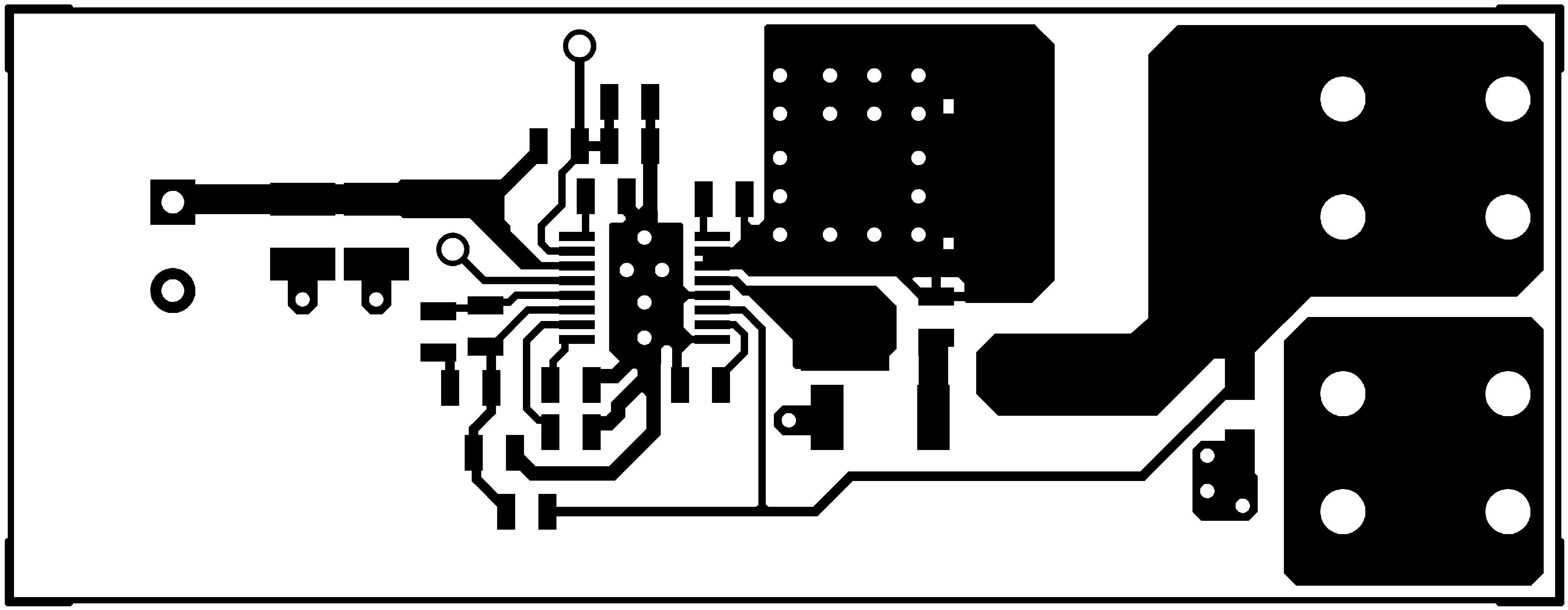
Figure 16.
Component Side
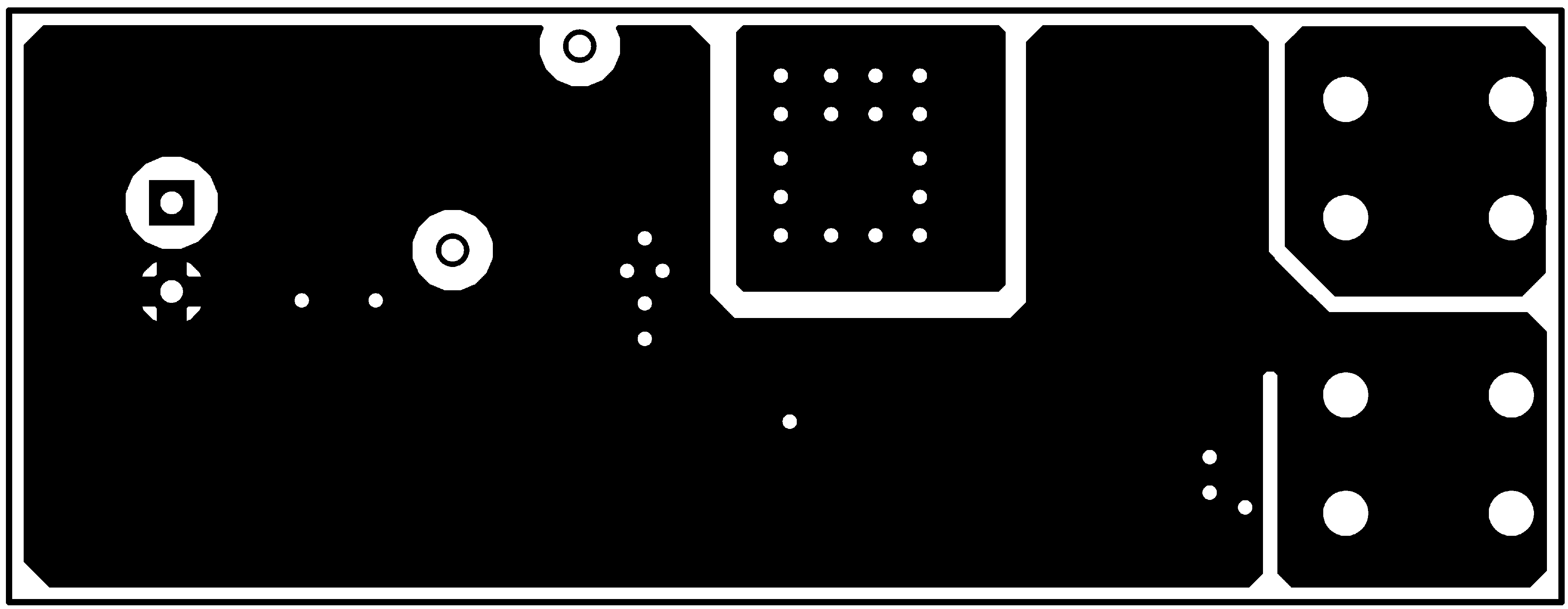
Figure 17.
Solder Side
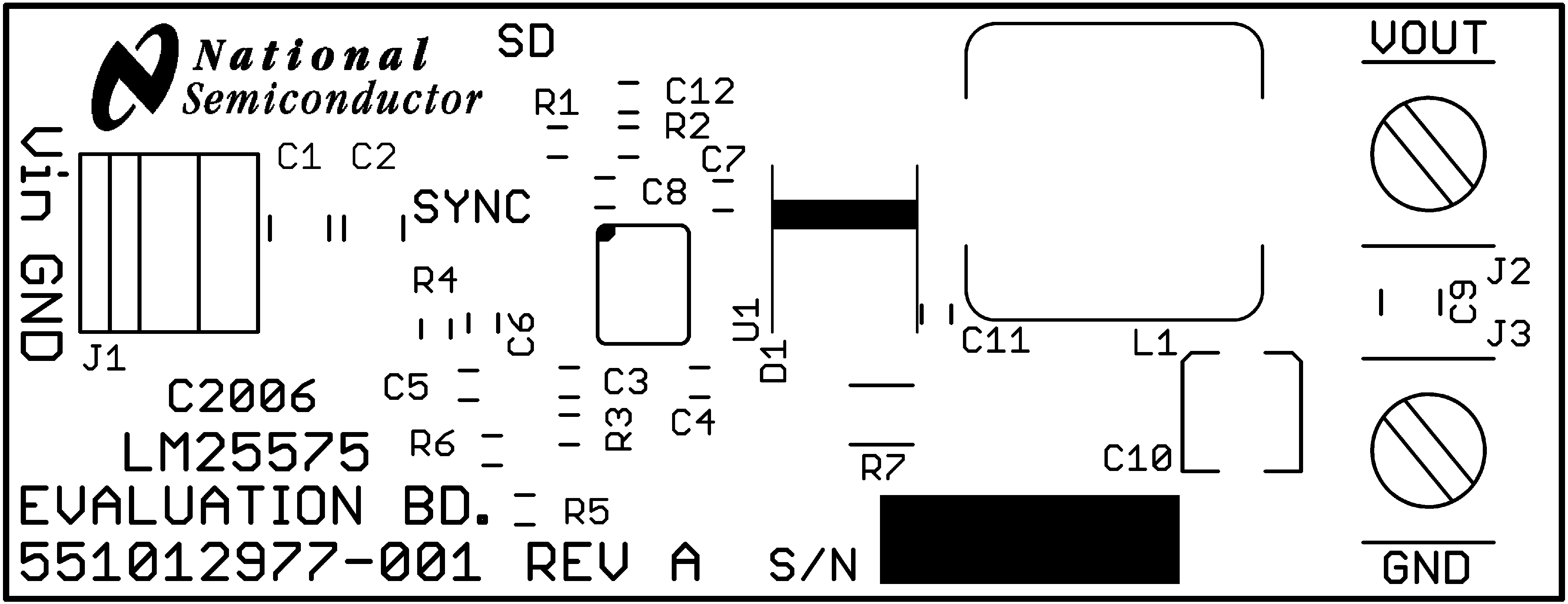
Figure 18.
Silkscreen