SNVS120G April 2000 – May 2019 LM2585
PRODUCTION DATA.
- 1 Features
- 2 Applications
- 3 Description
- 4 Revision History
- 5 Pin Configurations
-
6 Specifications
- 6.1 Absolute Maximum Ratings
- 6.2 ESD Ratings
- 6.3 Recommended Operating Ratings
- 6.4 Thermal Information
- 6.5 Electrical Characteristics: 3.3 V
- 6.6 Electrical Characteristics: 5 V
- 6.7 Electrical Characteristics: 12-V
- 6.8 Electrical Characteristics: Adjustable
- 6.9 Electrical Characteristics: All Versions
- 6.10 Typical Characteristics
- 7 Detailed Description
- 8 Application and Implementation
- 9 Layout
- 10Device and Documentation Support
- 11Mechanical, Packaging, and Orderable Information
Package Options
Mechanical Data (Package|Pins)
Thermal pad, mechanical data (Package|Pins)
- KTT|5
Orderable Information
9.2 Heat Sink/Thermal Considerations
In many cases, no heat sink is required to keep the LM2585 junction temperature within the allowed operating range. For each application, to determine whether or not a heat sink will be required, the following must be identified:
1) Maximum ambient temperature (in the application).
2) Maximum regulator power dissipation (in the application).
3) Maximum allowed junction temperature (125°C for the LM2585). For a safe, conservative design, a temperature approximately 15°C cooler than the maximum junction temperature should be selected (110°C).
4) LM2585 package thermal resistances θJA and θJC (given in Thermal Information).
Total power dissipated (PD) by the LM2585 can be estimated as follows:

where
- VIN is the minimum input voltage
- VOUT is the output voltage
- N is the transformer turns ratio
- D is the duty cycle
- ILOAD is the maximum load current (and ∑ILOAD is the sum of the maximum load currents for multiple-output flyback regulators)
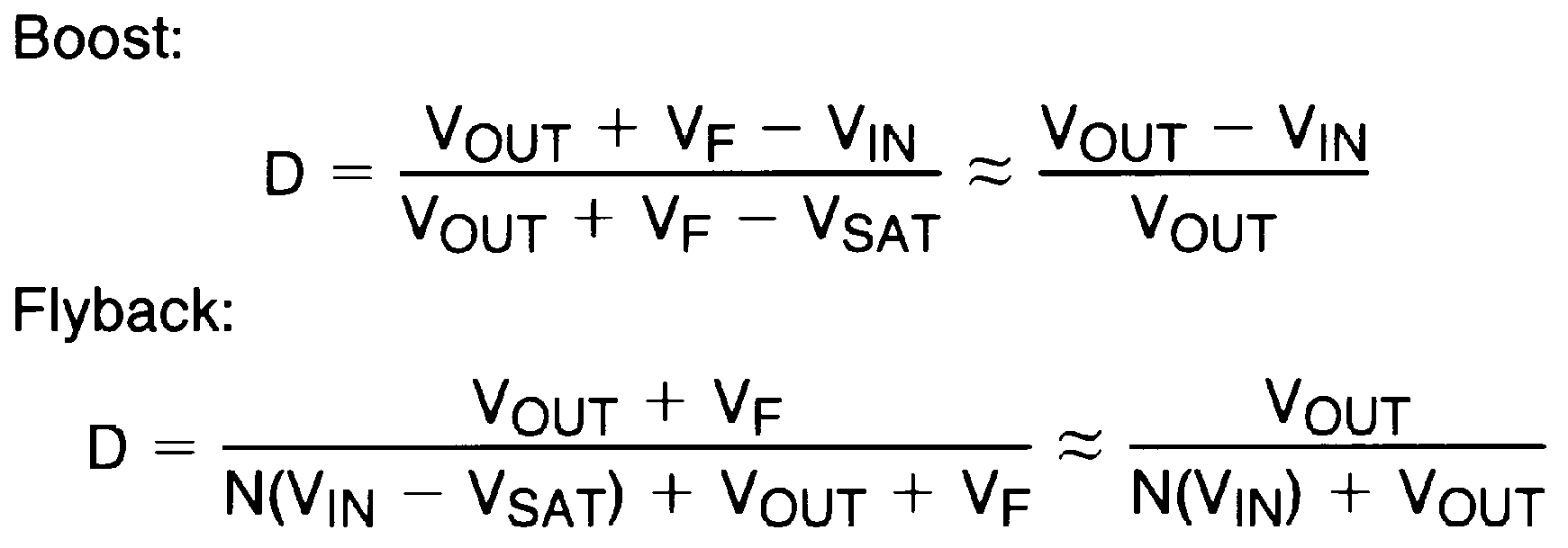
The duty cycle is given by:

where
- VF is the forward biased voltage of the diode and is typically 0.5V for Schottky diodes and 0.8V for fast recovery diodes
- VSAT is the switch saturation voltage and can be found in the Characteristic Curves
When no heat sink is used, the junction temperature rise is:
Adding the junction temperature rise to the maximum ambient temperature gives the actual operating junction temperature:
If the operating junction temperature exceeds the maximum junction temperatue in item 3 above, then a heat sink is required. When using a heat sink, the junction temperature rise can be determined by the following:
Again, the operating junction temperature will be:
As before, if the maximum junction temperature is exceeded, a larger heat sink is required (one that has a lower thermal resistance).
Included in the Switchers Made Simple design software is a more precise (non-linear) thermal model that can be used to determine junction temperature with different input-output parameters or different component values. It can also calculate the heat sink thermal resistance required to maintain the regulator junction temperature below the maximum operating temperature.