SNVS120G April 2000 – May 2019 LM2585
PRODUCTION DATA.
- 1 Features
- 2 Applications
- 3 Description
- 4 Revision History
- 5 Pin Configurations
-
6 Specifications
- 6.1 Absolute Maximum Ratings
- 6.2 ESD Ratings
- 6.3 Recommended Operating Ratings
- 6.4 Thermal Information
- 6.5 Electrical Characteristics: 3.3 V
- 6.6 Electrical Characteristics: 5 V
- 6.7 Electrical Characteristics: 12-V
- 6.8 Electrical Characteristics: Adjustable
- 6.9 Electrical Characteristics: All Versions
- 6.10 Typical Characteristics
- 7 Detailed Description
- 8 Application and Implementation
- 9 Layout
- 10Device and Documentation Support
- 11Mechanical, Packaging, and Orderable Information
Package Options
Mechanical Data (Package|Pins)
Thermal pad, mechanical data (Package|Pins)
- KTT|5
Orderable Information
8.2.4.3 Short Circuit Condition
Due to the inherent nature of boost regulators, when the output is shorted (Figure 50), current flows directly from the input, through the inductor and the diode, to the output, bypassing the switch. The current limit of the switch does not limit the output current for the entire circuit. To protect the load and prevent damage to the switch, the current must be externally limited, either by the input supply or at the output with an external current limit circuit. The external limit should be set to the maximum switch current of the device, which is 3A.
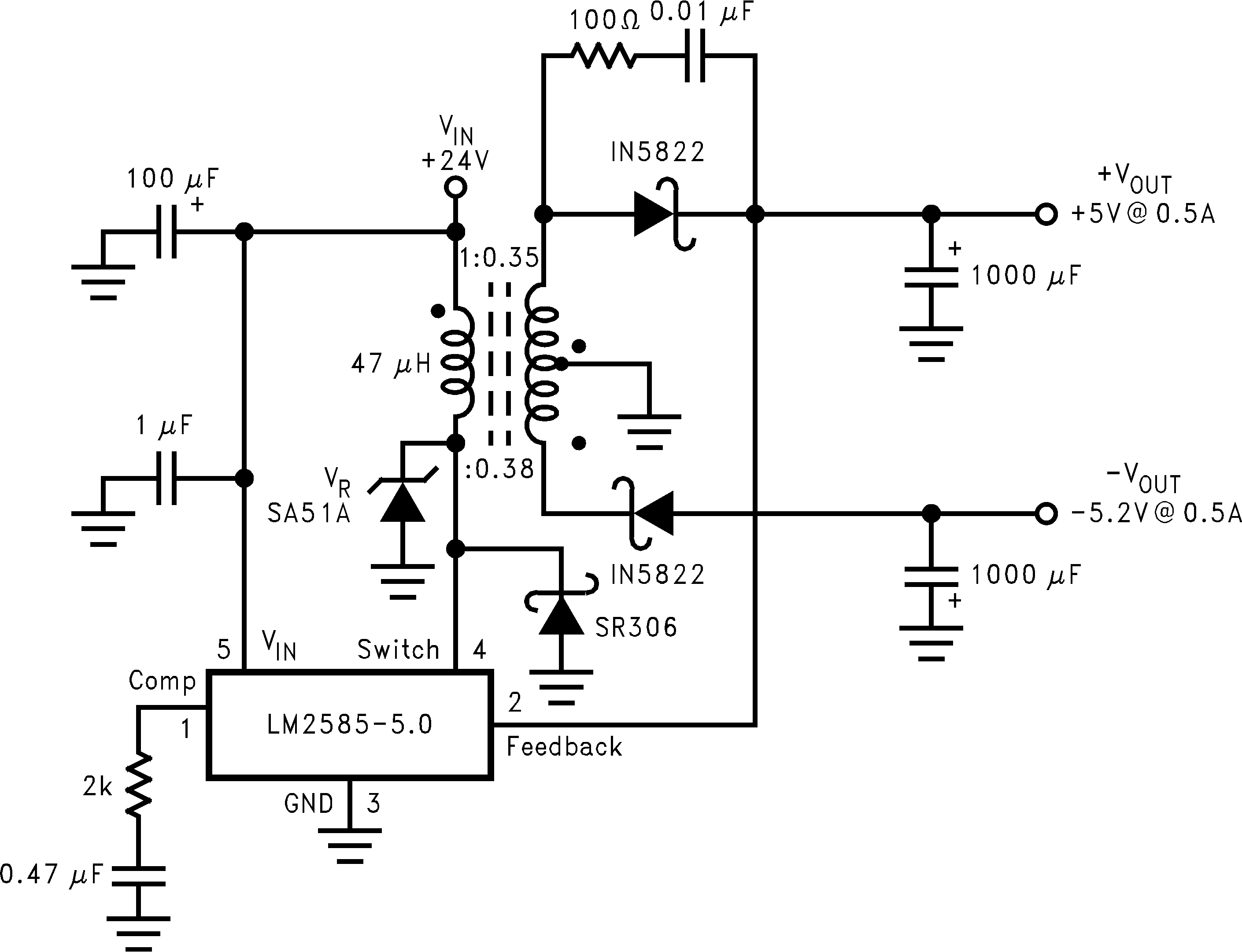
In a flyback regulator application (Figure 43), using the standard transformers, the LM2585 will survive a short circuit to the main output. When the output voltage drops to 80% of its nominal value, the frequency drops to 25 kHz. With a lower frequency, off times are larger. With the longer off times, the transformer can release all of its stored energy before the switch turns back on. Hence, the switch turns on initially with zero current at its collector. In this condition, the switch current limit will limit the peak current, saving the device.
 Figure 43. Flyback Regulator