SNVS117E April   1998  – June 2019 LM2588

PRODUCTION DATA.  

  1. Features
  2. Typical Applications
  3. Description
    1.     Device Images
      1.      Flyback Regulator
  4. Revision History
  5. Pin Configurations
  6. Specifications
    1. 6.1 Absolute Maximum Ratings
    2. 6.2 ESD Ratings
    3. 6.3 Recommended Operating Ratings
    4. 6.4 Electrical Characteristics: 3.3 V
    5. 6.5 Electrical Characteristics: 5 V
    6. 6.6 Electrical Characteristics: 12 V
    7. 6.7 Electrical Characteristics: Adjustable
    8. 6.8 Electrical Characteristics: All Output Voltage Versions
    9. 6.9 Typical Characteristics
  7. Detailed Description
    1. 7.1 Overview
    2. 7.2 Functional Block Diagram
    3. 7.3 Feature Description
      1. 7.3.1 Flyback Regulator Operation
      2. 7.3.2 Step-Up (Boost) Regulator Operation
      3. 7.3.3 Shutdown Control
      4. 7.3.4 Frequency Adjustment
      5. 7.3.5 Frequency Synchronization
      6. 7.3.6 Programming Output Voltage (Selecting R1 And R2)
      7. 7.3.7 Short-Circuit Condition
  8. Application and Implementation
    1. 8.1 Application Information
    2. 8.2 Typical Applications
      1. 8.2.1 Typical Flyback Regulator Applications
        1. 8.2.1.1 Design Requirements
          1. 8.2.1.1.1 Transformer Selection (T)
          2. 8.2.1.1.2 Transformer Footprints
        2. 8.2.1.2 Detailed Design Procedure
          1. 8.2.1.2.1 Custom Design With WEBENCH® Tools
          2. 8.2.1.2.2 Flyback Regulator Input Capacitors
          3. 8.2.1.2.3 Switch Voltage Limits
          4. 8.2.1.2.4 Output Voltage Limitations
          5. 8.2.1.2.5 Noisy Input Line Condition
          6. 8.2.1.2.6 Stability
      2. 8.2.2 Typical Boost Regulator Applications
        1. 8.2.2.1 Design Requirements
        2. 8.2.2.2 Detailed Design Procedure
    3. 8.3 System Examples
      1. 8.3.1 Test Circuits
  9. Layout
    1. 9.1 Layout Guidelines
    2. 9.2 Layout Example
    3. 9.3 Heat Sink/Thermal Considerations
  10. 10Device and Documentation Support
    1. 10.1 Device Support
      1. 10.1.1 Third-Party Products Disclaimer
      2. 10.1.2 Development Support
        1. 10.1.2.1 Custom Design With WEBENCH® Tools
    2. 10.2 Receiving Notification of Documentation Updates
    3. 10.3 Community Resources
    4. 10.4 Trademarks
    5. 10.5 Electrostatic Discharge Caution
    6. 10.6 Glossary
  11. 11Mechanical, Packaging, and Orderable Information

Package Options

Mechanical Data (Package|Pins)
Thermal pad, mechanical data (Package|Pins)
Orderable Information

Pin Configurations

NDZ Package
7-Pin TO-220
Top View, Bent, Staggered Leads
LM2588 01242017.png
KTW Package
7-Pin DDPAK/TO-263
Top View
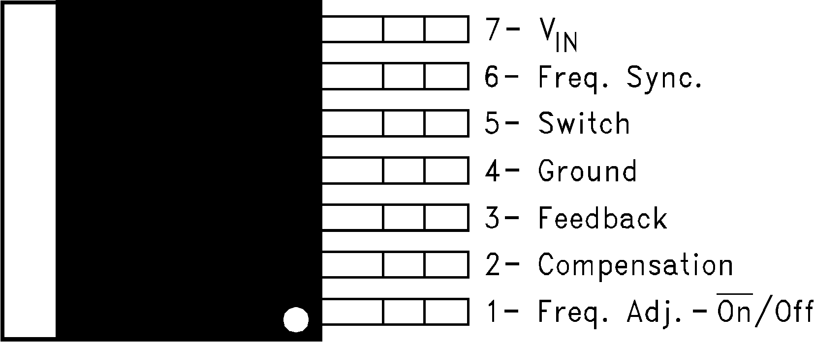
LM2588 01242019.png
NDZ Package
7-Pin TO-220
Side View; Bent, Staggered Leads
LM2588 01242018.png
KTW Package
7-Pin DDPAK/TO-263
Side View
LM2588 01242020.png