SNVS117E April   1998  – June 2019 LM2588

PRODUCTION DATA.  

  1. Features
  2. Typical Applications
  3. Description
    1.     Device Images
      1.      Flyback Regulator
  4. Revision History
  5. Pin Configurations
  6. Specifications
    1. 6.1 Absolute Maximum Ratings
    2. 6.2 ESD Ratings
    3. 6.3 Recommended Operating Ratings
    4. 6.4 Electrical Characteristics: 3.3 V
    5. 6.5 Electrical Characteristics: 5 V
    6. 6.6 Electrical Characteristics: 12 V
    7. 6.7 Electrical Characteristics: Adjustable
    8. 6.8 Electrical Characteristics: All Output Voltage Versions
    9. 6.9 Typical Characteristics
  7. Detailed Description
    1. 7.1 Overview
    2. 7.2 Functional Block Diagram
    3. 7.3 Feature Description
      1. 7.3.1 Flyback Regulator Operation
      2. 7.3.2 Step-Up (Boost) Regulator Operation
      3. 7.3.3 Shutdown Control
      4. 7.3.4 Frequency Adjustment
      5. 7.3.5 Frequency Synchronization
      6. 7.3.6 Programming Output Voltage (Selecting R1 And R2)
      7. 7.3.7 Short-Circuit Condition
  8. Application and Implementation
    1. 8.1 Application Information
    2. 8.2 Typical Applications
      1. 8.2.1 Typical Flyback Regulator Applications
        1. 8.2.1.1 Design Requirements
          1. 8.2.1.1.1 Transformer Selection (T)
          2. 8.2.1.1.2 Transformer Footprints
        2. 8.2.1.2 Detailed Design Procedure
          1. 8.2.1.2.1 Custom Design With WEBENCH® Tools
          2. 8.2.1.2.2 Flyback Regulator Input Capacitors
          3. 8.2.1.2.3 Switch Voltage Limits
          4. 8.2.1.2.4 Output Voltage Limitations
          5. 8.2.1.2.5 Noisy Input Line Condition
          6. 8.2.1.2.6 Stability
      2. 8.2.2 Typical Boost Regulator Applications
        1. 8.2.2.1 Design Requirements
        2. 8.2.2.2 Detailed Design Procedure
    3. 8.3 System Examples
      1. 8.3.1 Test Circuits
  9. Layout
    1. 9.1 Layout Guidelines
    2. 9.2 Layout Example
    3. 9.3 Heat Sink/Thermal Considerations
  10. 10Device and Documentation Support
    1. 10.1 Device Support
      1. 10.1.1 Third-Party Products Disclaimer
      2. 10.1.2 Development Support
        1. 10.1.2.1 Custom Design With WEBENCH® Tools
    2. 10.2 Receiving Notification of Documentation Updates
    3. 10.3 Community Resources
    4. 10.4 Trademarks
    5. 10.5 Electrostatic Discharge Caution
    6. 10.6 Glossary
  11. 11Mechanical, Packaging, and Orderable Information

Package Options

Mechanical Data (Package|Pins)
Thermal pad, mechanical data (Package|Pins)
Orderable Information

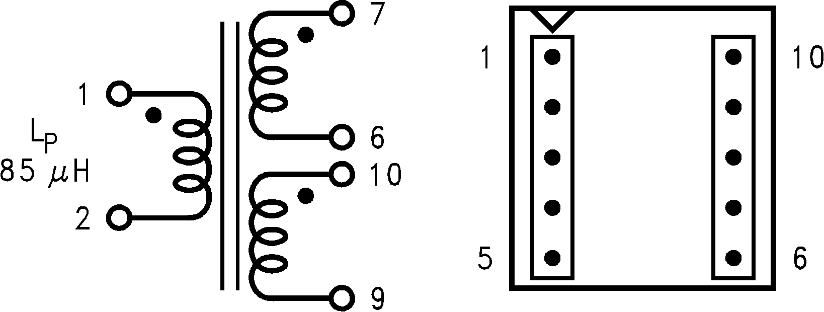
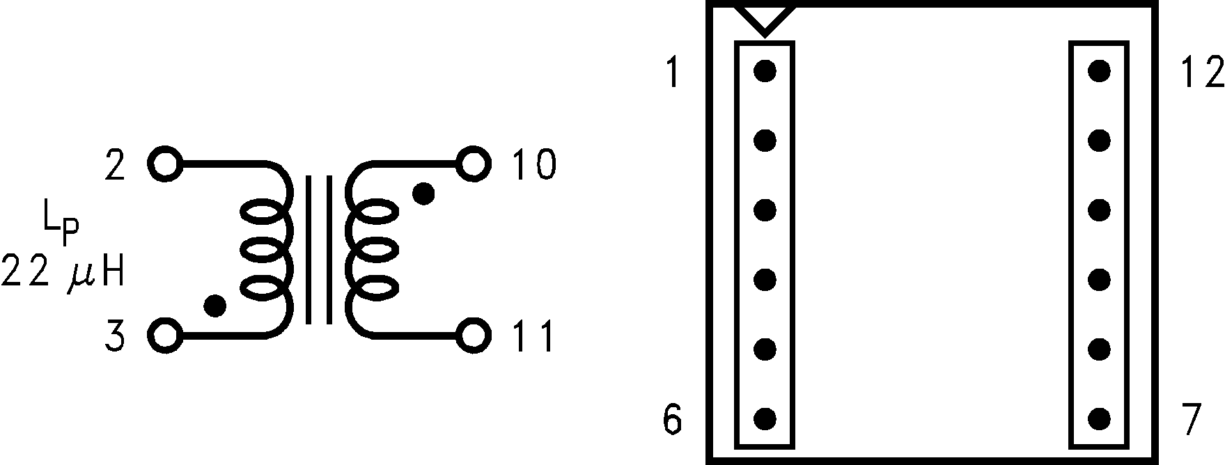
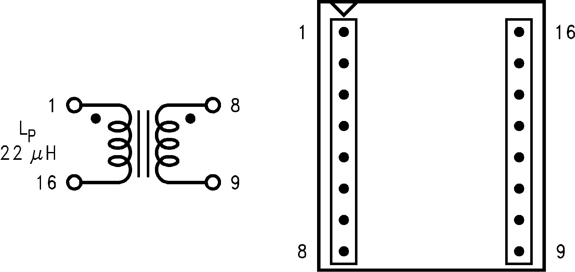
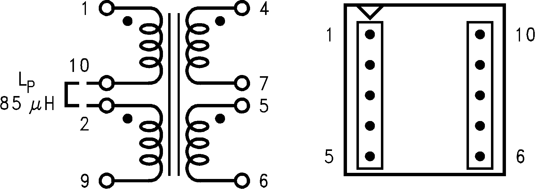
Transformer Footprints

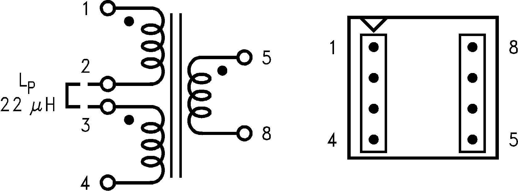
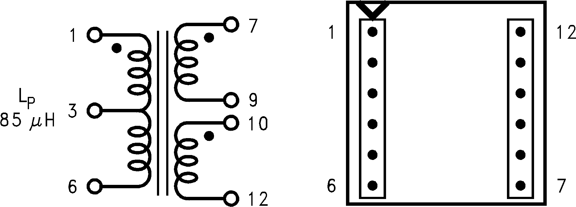
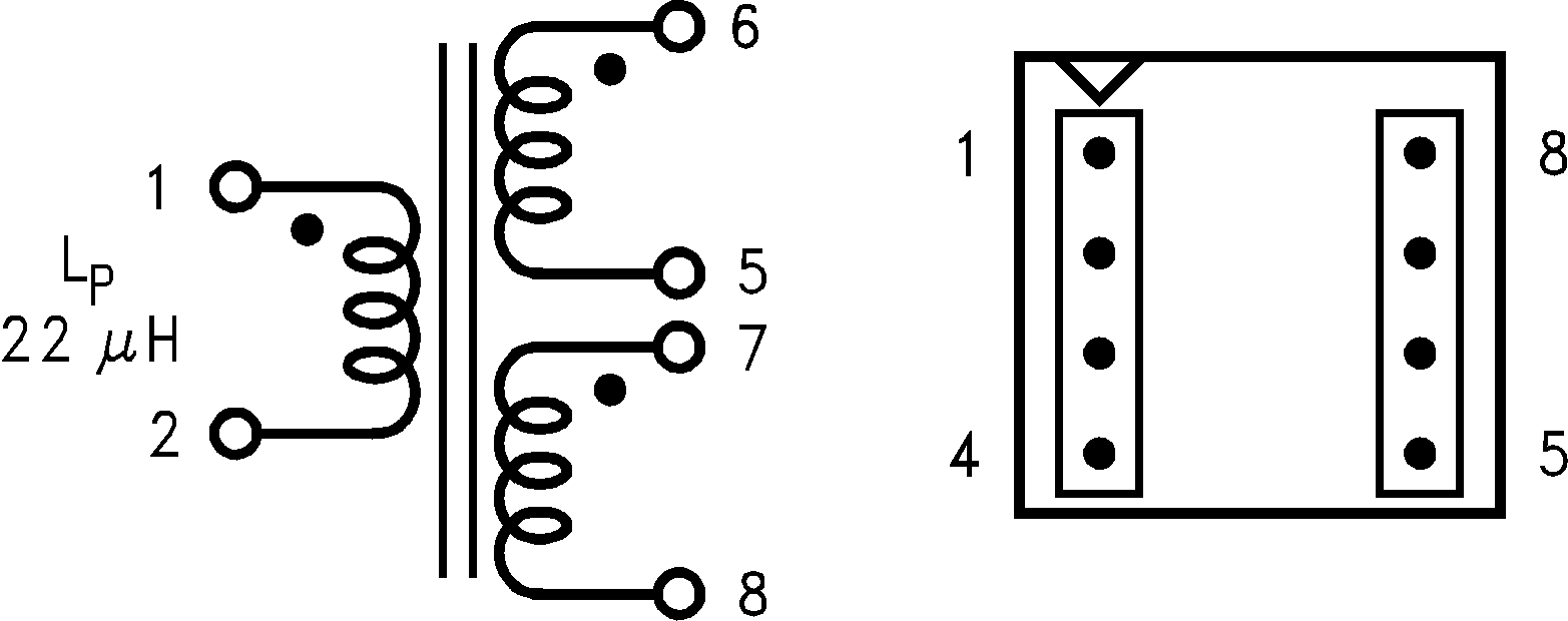
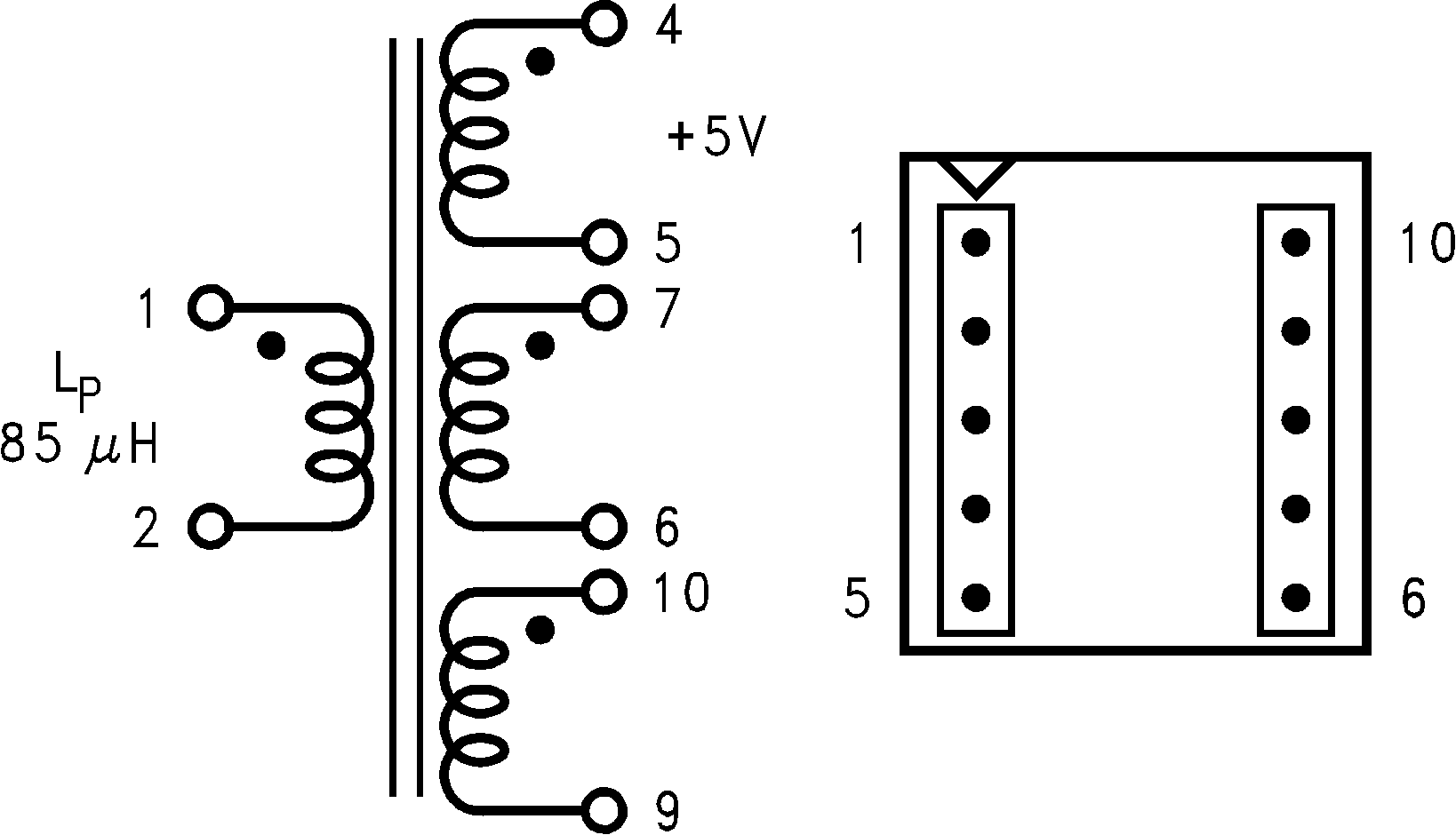
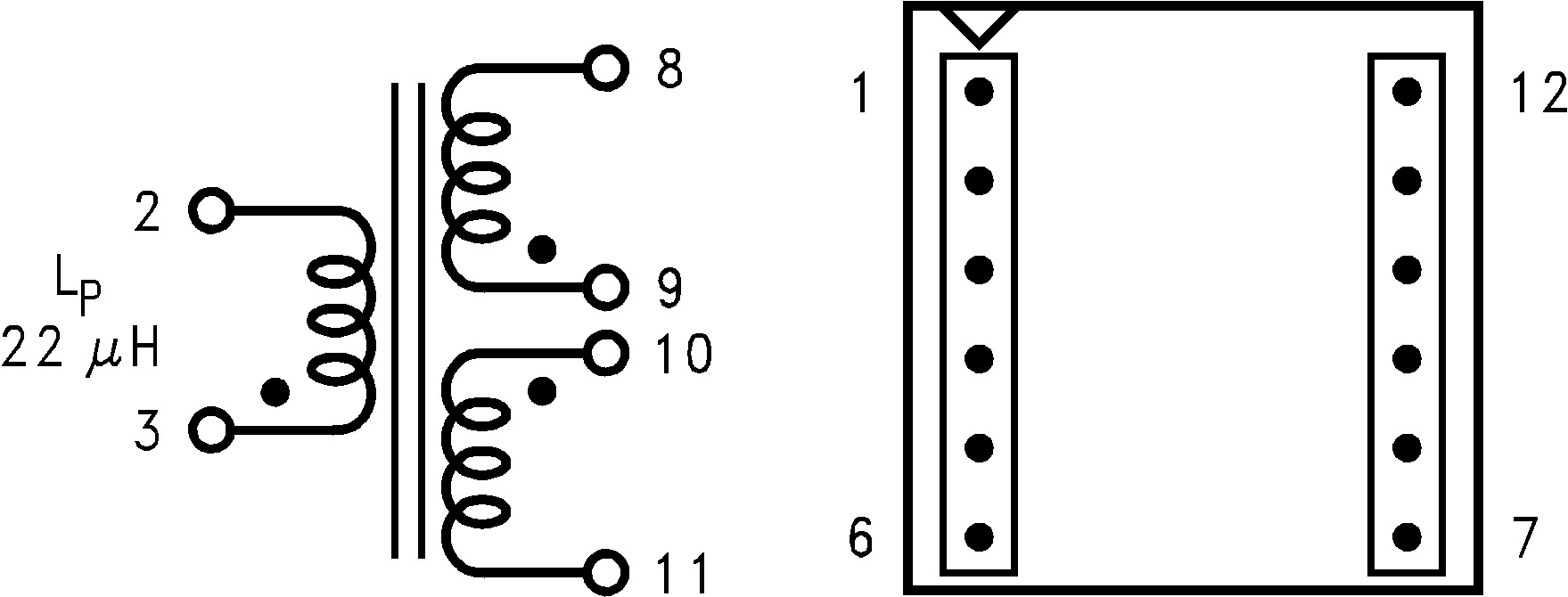
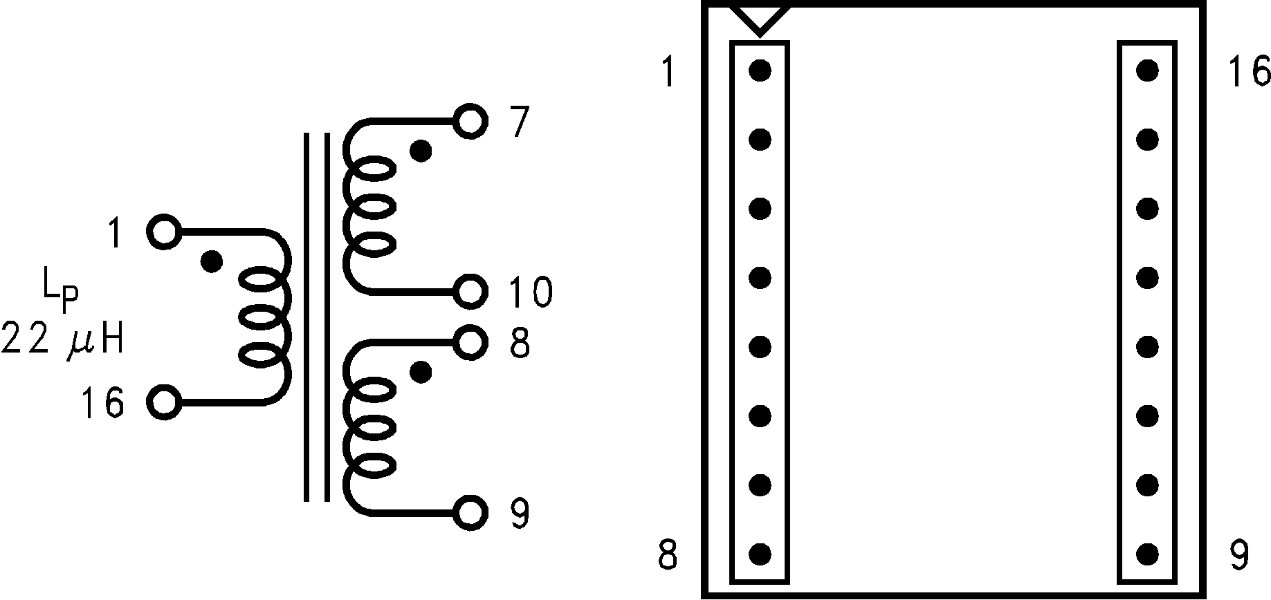
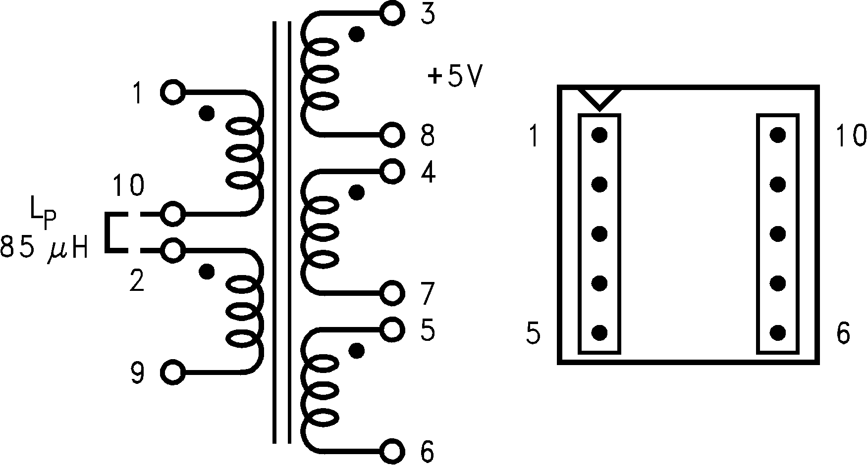
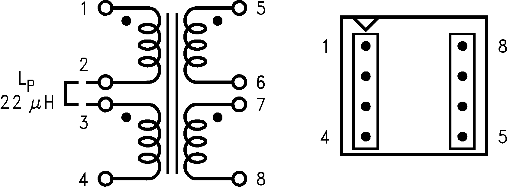
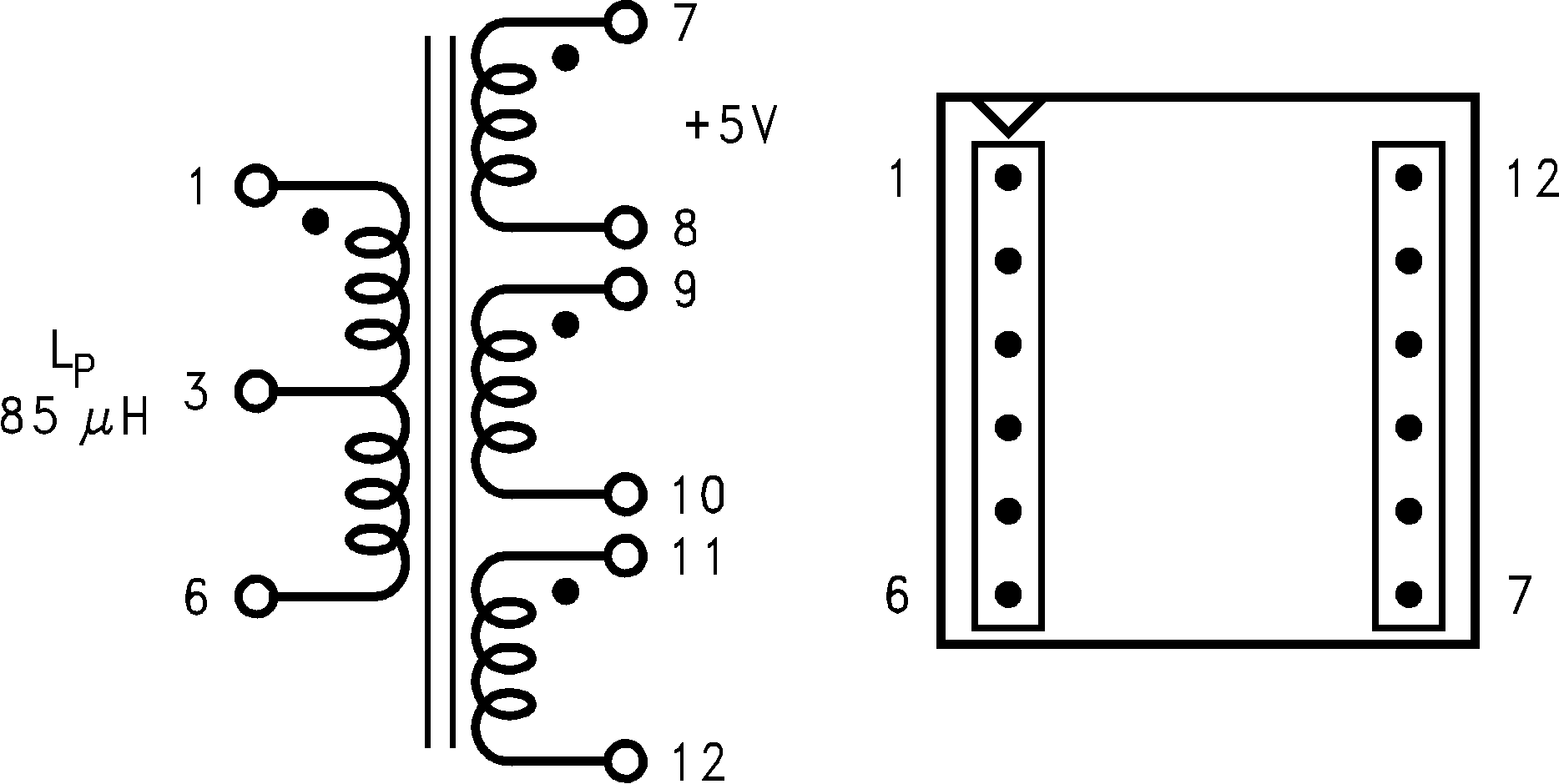
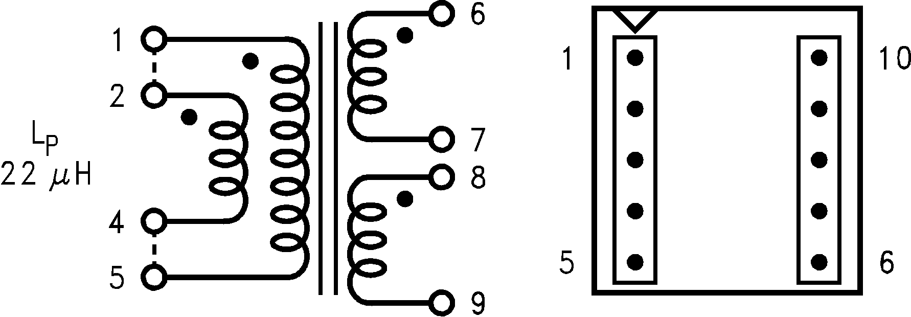
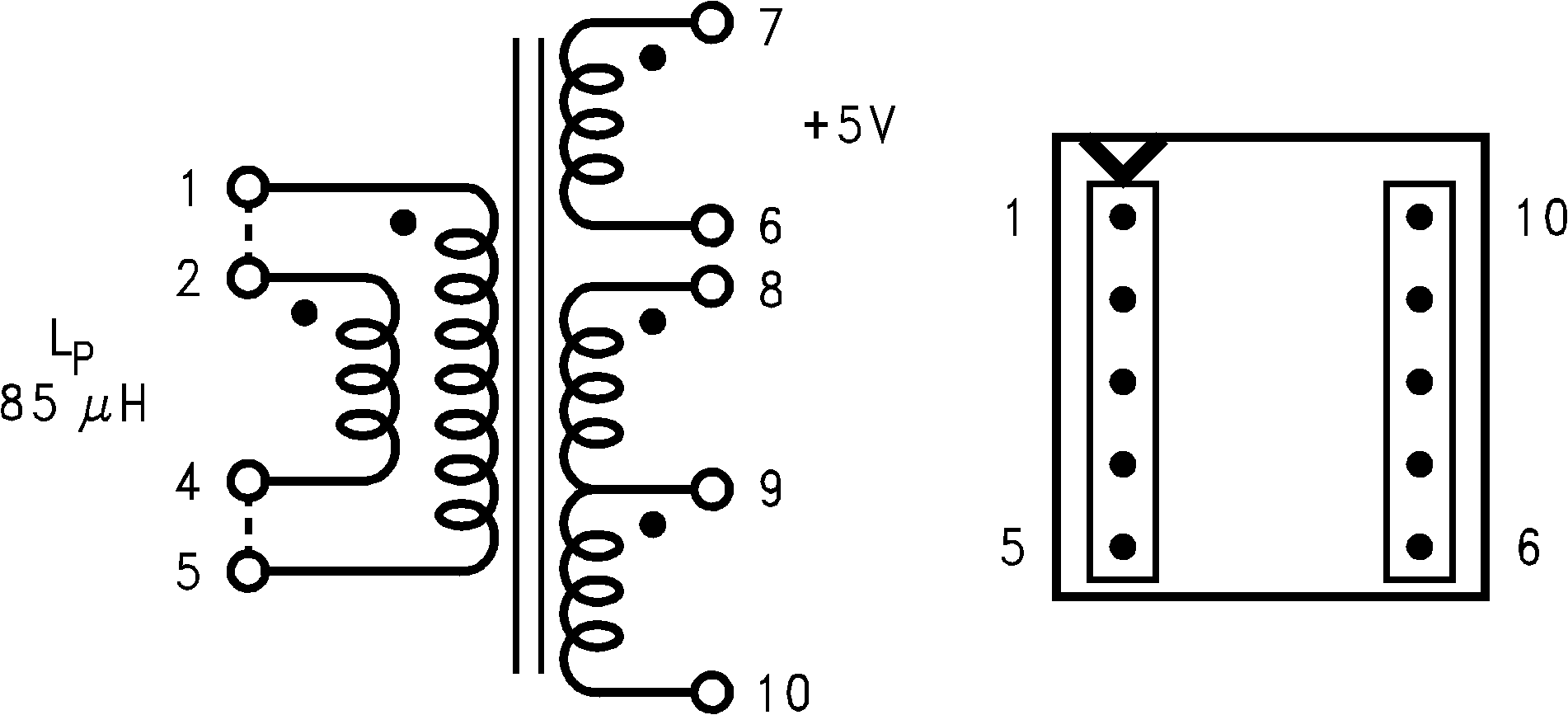
Figure 31 through Figure 48 show the footprints of each transformer, listed in Table 3.

LM2588 01242031.png
Figure 31. T1 - Top View
Coilcraft Q4434-B
LM2588 01242033.png
Figure 33. T3 - Top View
Coilcraft Q4343-B
LM2588 01242035.png
Figure 35. T1 - Top View
Coilcraft Q4435-B
(Surface Mount)
LM2588 01242037.png
Figure 37. T1 - Top View
Pulse PE-68411
(Surface Mount)
LM2588 01242039.png
Figure 39. T3 - Top View
Pulse PE-68421
(Surface Mount)
LM2588 01242041.png
Figure 41. T1 - Top View
Renco RL-5530
LM2588 01242043.png
Figure 43. T3 - Top View
Renco RL-5534
LM2588 01242045.png
Figure 45. T1 - Top View
Schott 67141450
LM2588 01242047.png
Figure 47. T3 - Top View
Schott 67140920
LM2588 01242032.png
Figure 32. T2 - Top View
Coilcraft Q4337-B
LM2588 01242034.png
Figure 34. T4 - Top View
Coilcraft Q4344-B
LM2588 01242036.png
Figure 36. T2 - Top View
Coilcraft Q4436-B
(Surface Mount)
LM2588 01242038.png
Figure 38. T2 - Top View
Pulse PE-68412
(Surface Mount)
LM2588 01242040.png
Figure 40. T4 - Top View
Pulse PE-68422
(Surface Mount)
LM2588 01242042.png
Figure 42. T2 - Top View
Renco RL-5531
LM2588 01242044.png
Figure 44. T4 - Top View
Renco RL-5535
LM2588 01242046.png
Figure 46. T2 - Top View
Schott 67140860
LM2588 01242048.png
Figure 48. T4 - Top View
Schott 67140930