SNVS118F december 1999 – may 2023 LM2594 , LM2594HV
PRODUCTION DATA
- 1
- 1 Features
- 2 Applications
- 3 Description
- 4 Revision History
- 5 Description (continued)
- 6 Pin Configuration and Functions
-
7 Specifications
- 7.1 Absolute Maximum Ratings
- 7.2 ESD Ratings
- 7.3 Recommended Operating Conditions
- 7.4 Thermal Information
- 7.5 Electrical Characteristics – 3.3 V
- 7.6 Electrical Characteristics – 5 V
- 7.7 Electrical Characteristics – 12 V
- 7.8 Electrical Characteristics – Adjustable
- 7.9 Electrical Characteristics – All Output Voltage Versions
- 7.10 Typical Characteristics
- 8 Detailed Description
- 9 Application and Implementation
- 10Device and Documentation Support
- 11Mechanical, Packaging, and Orderable Information
Package Options
Mechanical Data (Package|Pins)
Thermal pad, mechanical data (Package|Pins)
Orderable Information
9.4.3 Thermal Considerations
The LM2594xx is available in two packages: an 8-pin through-hole PDIP and an 8-pin surface-mount SOIC. Both packages are molded plastic with a copper lead frame. When the package is soldered to the printed-circuit board (PCB), the copper and the board are the heat sink for the LM2594 and the other heat producing components.
For best thermal performance, wide copper traces must be used and all ground and unused pins must be soldered to generous amounts of PCB copper, such as a ground plane (one exception to this is the output (switch pin, which must not have large areas of copper). Large areas of copper provide the best transfer of heat (lower thermal resistance) to the surrounding air, and even double-sided or multilayer boards provide a better heat path to the surrounding air. Unless power levels are small, sockets are not recommended because of the added thermal resistance it adds and the resultant higher junction temperatures.
Package thermal resistance and junction temperature rise numbers are all approximate, and there are many factors that affects the junction temperature. Some of these factors include board size, shape, thickness, position, location, and even board temperature. Other factors are trace width, printed-circuit copper area, copper thickness, single- or double-sided multilayer board, and the amount of solder on the board. The effectiveness of the PCB to dissipate heat also depends on the size, quantity, and spacing of other components on the board. Furthermore, some of these components such as the catch diode adds heat to the PCB and the heat can vary as the input voltage changes. For the inductor, depending on the physical size, type of core material, and the DC resistance, it can either act as a heat sink taking heat away from the board, or it can add heat to the board.

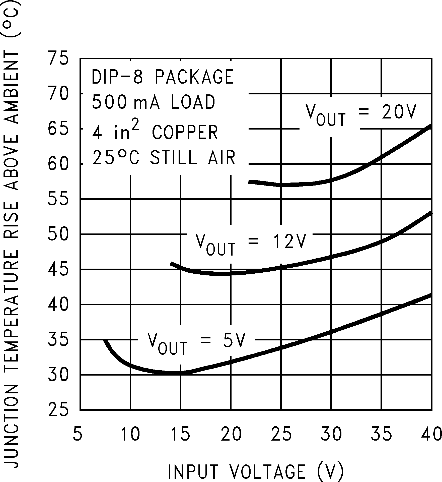
| Circuit Data for Temperature Rise Curve (8-Pin PDIP) | |
| Capacitors | Through hole electrolytic |
| Inductor | Through hole, Schott, 100 μH |
| Diode | Through hole, 1-A, 40-V, Schottky |
| PCB | 4 square inches single sided 2 oz. copper (0.0028″) |

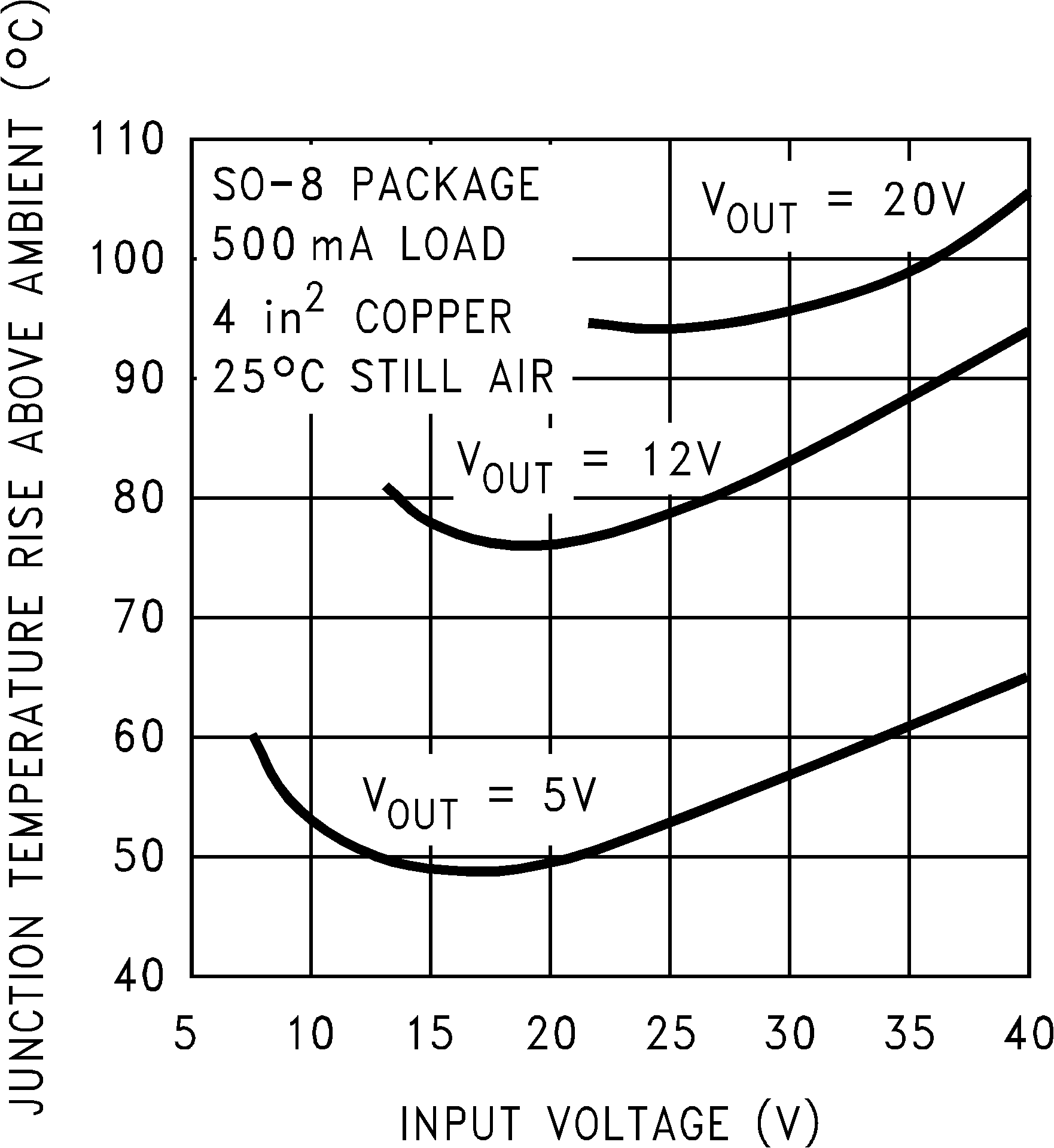
| Circuit Data for Temperature Rise Curve (Surface Mount) | |
| Capacitors | Surface mount tantalum, molded D size |
| Inductor | Surface mount, Coilcraft DO33, 100 μH |
| Diode | Surface mount, 1-A, 40-V, Schottky |
| PCB | 4 square inches single sided 2 oz. copper (0.0028″) |
Figure 9-18 and Figure 9-19 show the LM2594 junction temperature rise above ambient temperature with a 500-mA load for various input and output voltages. This data was taken with the circuit operating as a buck switcher with all components mounted on a PCB to simulate the junction temperature under actual operating conditions. This curve is typical, and can be used for a quick check on the maximum junction temperature for various conditions, but keep in mind that there are many factors that can affect the junction temperature.