SNVS118F december 1999 – may 2023 LM2594 , LM2594HV
PRODUCTION DATA
- 1
- 1 Features
- 2 Applications
- 3 Description
- 4 Revision History
- 5 Description (continued)
- 6 Pin Configuration and Functions
-
7 Specifications
- 7.1 Absolute Maximum Ratings
- 7.2 ESD Ratings
- 7.3 Recommended Operating Conditions
- 7.4 Thermal Information
- 7.5 Electrical Characteristics – 3.3 V
- 7.6 Electrical Characteristics – 5 V
- 7.7 Electrical Characteristics – 12 V
- 7.8 Electrical Characteristics – Adjustable
- 7.9 Electrical Characteristics – All Output Voltage Versions
- 7.10 Typical Characteristics
- 8 Detailed Description
- 9 Application and Implementation
- 10Device and Documentation Support
- 11Mechanical, Packaging, and Orderable Information
Package Options
Mechanical Data (Package|Pins)
Thermal pad, mechanical data (Package|Pins)
Orderable Information
8.4.1 Discontinuous Mode Operation
The selection guide chooses inductor values suitable for continuous mode operation, but for low current applications and high input voltages, a discontinuous mode design can be a better choice. Discontinuous mode can use an inductor that is physically smaller, and can need only one half to one third of the inductance value needed for a continuous mode design. The peak switch and inductor currents are higher in a discontinuous design, but at these low load currents (200 mA and below), the maximum switch current is still less than the switch current limit.
Discontinuous operation can have voltage waveforms that are considerably different than a continuous design. The output pin (switch) waveform can have some damped sinusoidal ringing present (see Figure 9-11). This ringing is normal for discontinuous operation, and is not caused by feedback loop instabilities. In discontinuous operation, there is a period of time where neither the switch nor the diode are conducting, and the inductor current has dropped to zero. During this time, a small amount of energy can circulate between the inductor and the switch or diode parasitic capacitance causing this characteristic ringing. Normally this ringing is not a problem, unless the amplitude becomes great enough to exceed the input voltage, and even then, there is very little energy present to cause damage.
Different inductor types and core materials produce different amounts of this characteristic ringing. Ferrite core inductors have very little core loss and, therefore, produce the most ringing. The higher core loss of powdered iron inductors produce less ringing. If desired, a series RC can be placed in parallel with the inductor to dampen the ringing.
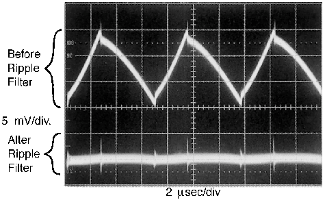
 Figure 8-9 Post Ripple Filter Waveform