-
LM2599 SIMPLE SWITCHER® Power Converter 150-kHz 3-A Step-Down Voltage Regulator, With Features
- 1 Features
- 2 Applications
- 3 Description
- 4 Revision History
- 5 Description (continued)
- 6 Pin Configuration and Functions
-
7 Specifications
- 7.1 Absolute Maximum Ratings
- 7.2 ESD Ratings
- 7.3 Recommended Operating Conditions
- 7.4 Thermal Information
- 7.5 Electrical Characteristics - 3.3-V Version
- 7.6 Electrical Characteristics - 5-V Version
- 7.7 Electrical Characteristics - 12-V Version
- 7.8 Electrical Characteristics - Adjustable Voltage Version
- 7.9 Electrical Characteristics - All Output Voltage Versions
- 7.10 Typical Characteristics
- 8 Detailed Description
-
9 Application and Implementation
- 9.1
Application Information
- 9.1.1 Soft-Start Capacitor (CSS)
- 9.1.2 Delay Capacitor (CDELAY)
- 9.1.3 Feedforward Capacitor (CFF) for Adjustable Output Voltage Version Only
- 9.1.4 Input Capacitor (CIN)
- 9.1.5 Output Capacitor (COUT)
- 9.1.6 Catch Diode
- 9.1.7 Inductor Selection
- 9.1.8 Output Voltage Ripple and Transients
- 9.1.9 Open Core Inductors
- 9.2 Typical Applications
- 9.1
Application Information
- 10Power Supply Recommendations
- 11Layout
- 12Device and Documentation Support
- 13Mechanical, Packaging, and Orderable Information
- IMPORTANT NOTICE
Package Options
Mechanical Data (Package|Pins)
Thermal pad, mechanical data (Package|Pins)
- KTW|7
Orderable Information
LM2599 SIMPLE SWITCHER® Power Converter 150-kHz 3-A Step-Down Voltage Regulator, With Features
1 Features
- 3.3-V, 5-V, 12-V, and Adjustable Output Versions
- Adjustable Version Output Voltage Range: 1.2 V to 37 V ±4% Maximum Over Line and Load Conditions
- 3-A Output Current
- Available in 7-Pin TO-220 and TO-263 (Surface-Mount) Package
- Input Voltage Range Up to 40 V
- 150-kHz Fixed-Frequency Internal Oscillator
- Shutdown and Soft-Start
- Out-of-Regulation Error Flag
- Error Output Delay
- Low Power Standby Mode, IQ, Typically 80 μA
- High Efficiency
- Uses Readily Available Standard Inductors
- Thermal Shutdown and Current-Limit Protection
2 Applications
- Simple High-Efficiency Step-Down (Buck) Regulator
- Efficient Preregulator for Linear Regulators
- On-Card Switching Regulators
- Positive to Negative Converter
3 Description
The LM2599 series of regulators are monolithic integrated circuits that provide all the active functions for a step-down (buck) switching regulator, capable of driving a 3-A load with excellent line and load regulation. These devices are available in fixed output voltages of 3.3 V, 5 V, 12 V, and an adjustable output version.
The LM2598 is a member of the LM259x family, with additional supervisory and performance features added.
Requiring a minimum number of external components, these regulators are simple to use and include internal frequency compensation, improved line and load specifications, fixed-frequency oscillator, Shutdown and Soft-start, error flag delay, and error flag output.
Device Information(1)
| PART NUMBER | PACKAGE | BODY SIZE (NOM) |
|---|---|---|
| LM2599 | TO-220 (7) | 14.986 mm × 10.16 mm |
| TO-263 (7) | 10.10 mm × 8.89 mm |
- For all available packages, see the orderable addendum at the end of the data sheet.
Typical Application

4 Revision History
Changes from C Revision (April 2013) to D Revision
- Added ESD Ratings table, Feature Description section, Device Functional Modes, Application and Implementation section, Power Supply Recommendations section, Layout section, Device and Documentation Support section, and Mechanical, Packaging, and Orderable Information section.Go
- Removed all references to design software Switchers Made Simple Go
Changes from B Revision (April 2013) to C Revision
- Changed layout of National Semiconductor Data Sheet to TI formatGo
5 Description (continued)
The LM2599 series operates at a switching frequency of 150 kHz, thus allowing smaller sized filter components than what would be needed with lower frequency switching regulators. Available in a standard 7-pin TO-220 package with several different lead bend options, and a 7-pin TO-263 surface-mount package.
A standard series of inductors (both through-hole and surface-mount types) are available from several different manufacturers optimized for use with the LM2599 series. This feature greatly simplifies the design of switch-mode power supplies.
Other features include a ±4% tolerance on output voltage under all conditions of input voltage and output load conditions, and ±15% on the oscillator frequency. External shutdown is included, featuring typically 80-μA standby current. Self-protection features include a two stage current limit for the output switch and an overtemperature shutdown for complete protection under fault conditions.
6 Pin Configuration and Functions


Pin Functions(1)
| PIN | I/O | DESCRIPTION | |
|---|---|---|---|
| NO. | NAME | ||
| 1 | +VIN | I | This is the positive input supply for the IC switching regulator. A suitable input bypass capacitor must be present at this pin to minimize voltage transients and to supply the switching currents needed by the regulator. |
| 2 | Output | O | Internal switch. The voltage at this pin switches between approximately (+VIN − VSAT) and approximately −0.5 V, with a duty cycle of VOUT/VIN. To minimize coupling to sensitive circuitry, the PCB copper area connected to this pin must be kept to a minimum. |
| 3 | Error Flag | O | Open-collector output that provides a low signal (flag transistor ON) when the regulated output voltage drops more than 5% from the nominal output voltage. On start up, Error Flag is low until VOUT reaches 95% of the nominal output voltage and a delay time determined by the Delay pin capacitor. This signal can be used as a reset to a microprocessor on power-up. |
| 4 | Ground | — | Circuit ground. |
| 5 | Delay | O | At power-up, this pin can be used to provide a time delay between the time the regulated output voltage reaches 95% of the nominal output voltage, and the time the error flag output goes high. |
| 6 | Feedback | I | Senses the regulated output voltage to complete the feedback loop. |
| 7 | Shutdown/Soft-start | I | This dual function pin provides the following features: (a) Allows the switching regulator circuit to be shut down using logic level signals thus dropping the total input supply current to approximately 80 μA. (b) Adding a capacitor to this pin provides a soft-start feature which minimizes start-up current and provides a controlled ramp up of the output voltage. |
7 Specifications
7.1 Absolute Maximum Ratings (1)(2)
| MIN | MAX | UNIT | |||
|---|---|---|---|---|---|
| Maximum supply voltage, VIN | 45 | V | |||
| SD/SS pin input voltage(3) | 6 | V | |||
| Delay pin voltage(3) | 1.5 | V | |||
| Flag pin voltage | –0.3 | 45 | V | ||
| Feedback pin voltage | –0.3 | 25 | V | ||
| Output voltage to ground (steady-state) | –1 | V | |||
| Power dissipation | Internally limited | ||||
| Lead temperature | KTW package | Vapor phase (60 s) | 215 | °C | |
| Infrared (10 s) | 245 | ||||
| NDZ package (soldering, 10 s) | 260 | ||||
| Maximum junction temperature | 150 | °C | |||
| Storage temperature, Tstg | −65 | 150 | °C | ||
7.2 ESD Ratings
| VALUE | UNIT | |||
|---|---|---|---|---|
| V(ESD) | Electrostatic discharge | Human-body model (HBM), per ANSI/ESDA/JEDEC JS-001(1) | ±2000 | V |
7.3 Recommended Operating Conditions
| MIN | MAX | UNIT | |
|---|---|---|---|
| Supply voltage | 4.5 | 40 | V |
| Temperature | –40 | 125 | °C |
7.4 Thermal Information
| THERMAL METRIC(1) | LM2599 | UNIT | |||
|---|---|---|---|---|---|
| KTW (TO-263) | NDZ (TO-220) | ||||
| 7 PINS | 7 PINS | ||||
| RθJA | Junction-to-ambient thermal resistance(2)(3) | See(4) | — | 50 | °C/W |
| See(5) | 50 | — | |||
| See(6) | 30 | — | |||
| See(7) | 20 | — | |||
| RθJC(top) | Junction-to-case (top) thermal resistance | 2 | 2 | °C/W | |
7.5 Electrical Characteristics – 3.3-V Version
Specifications are for TJ = 25°C (unless otherwise noted).| PARAMETER | TEST CONDITIONS | MIN(1) | TYP(2) | MAX (1) | UNIT | ||
|---|---|---|---|---|---|---|---|
| SYSTEM PARAMETERS(3) (see Figure 43 for test circuit) | |||||||
| VOUT | Output voltage | 4.75 V ≤ VIN ≤ 40 V, 0.2 A ≤ ILOAD ≤ 3 A |
TJ = 25°C | 3.168 | 3.3 | 3.432 | V |
| –40°C ≤ TJ ≤ 125°C | 3.135 | 3.465 | |||||
| η | Efficiency | VIN = 12 V, ILOAD = 3 A | 73% | ||||
7.6 Electrical Characteristics – 5-V Version
Specifications are for TJ = 25°C (unless otherwise noted).| PARAMETER | TEST CONDITIONS | MIN(1) | TYP(2) | MAX(1) | UNIT | ||
|---|---|---|---|---|---|---|---|
| SYSTEM PARAMETERS(3) (see Figure 43 for test circuit) | |||||||
| VOUT | Output voltage | 7 V ≤ VIN ≤ 40 V, 0.2 A ≤ ILOAD ≤ 3 A |
TJ = 25°C | 4.8 | 5 | 5.2 | V |
| –40°C ≤ TJ ≤ 125°C | 4.75 | 5.25 | |||||
| η | Efficiency | VIN = 12 V, ILOAD = 3 A | 80% | ||||
7.7 Electrical Characteristics – 12-V Version
Specifications are for TJ = 25°C (unless otherwise noted).| PARAMETER | TEST CONDITIONS | MIN(1) | TYP(2) | MAX(1) | UNIT | ||
|---|---|---|---|---|---|---|---|
| SYSTEM PARAMETERS(3) (see Figure 43 for test circuit) | |||||||
| VOUT | Output voltage | 15 V ≤ VIN ≤ 40 V, 0.2 A ≤ ILOAD ≤ 3 A |
TJ = 25°C | 11.52 | 12 | 12.48 | V |
| –40°C ≤ TJ ≤ 125°C | 11.4 | 12.6 | |||||
| η | Efficiency | VIN = 25 V, ILOAD = 3 A | 90% | ||||
7.8 Electrical Characteristics – Adjustable Voltage Version
Specifications are for TJ = 25°C (unless otherwise noted).| PARAMETER | TEST CONDITIONS | MIN(1) | TYP(2) | MAX(1) | UNIT | ||
|---|---|---|---|---|---|---|---|
| SYSTEM PARAMETERS(3) (see Figure 43 for test circuit) | |||||||
| VFB | Feedback voltage | 4.5 V ≤ VIN ≤ 40 V, 0.2 A ≤ ILOAD ≤ 3 A | 1.23 | V | |||
| VOUT programmed for 3 V, circuit of Figure 43 |
TJ = 25°C | 1.193 | 1.267 | ||||
| –40°C ≤ TJ ≤ 125°C | 1.18 | 1.28 | |||||
| η | Efficiency | VIN = 12 V, VOUT = 3 V, ILOAD = 3 A | 73% | ||||
7.9 Electrical Characteristics – All Output Voltage Versions
Specifications are for TJ = 25°C, ILOAD = 500 mA, VIN = 12 V for the 3.3-V, 5-V, and Adjustable version, and VIN = 24 V for the 12-V version (unless otherwise noted).| PARAMETER | TEST CONDITIONS | MIN(1) | TYP(2) | MAX(1) | UNIT | ||
|---|---|---|---|---|---|---|---|
| DEVICE PARAMETERS | |||||||
| Ib | Feedback bias current | Adjustable voltage version only, VFB = 1.3 V | TJ = 25°C | 10 | 50 | nA | |
| –40°C ≤ TJ ≤ 125°C | 100 | ||||||
| fO | Oscillator frequency(3) | TJ = 25°C | 127 | 150 | 173 | kHz | |
| –40°C ≤ TJ ≤ 125°C | 110 | 173 | |||||
| VSAT | Saturation voltage | IOUT = 3 A(4)(5) | TJ = 25°C | 1.16 | 1.4 | V | |
| –40°C ≤ TJ ≤ 125°C | 1.5 | ||||||
| DC | Max duty cycle (ON)(5) | 100% | |||||
| Min duty cycle (OFF)(6) | 0% | ||||||
| ICL | Current limit | Peak current(4) (5) | TJ = 25°C | 3.6 | 4.5 | 6.9 | A |
| –40°C ≤ TJ ≤ 125°C | |||||||
| 3.4 | 7.5 | ||||||
| IL | Output leakage current | Output = 0 V, VIN = 40 V(4) (6) | 50 | μA | |||
| Output = −1 V | 2 | 30 | mA | ||||
| IQ | Operating quiescent current | SD/SS pin open(6) | 5 | 10 | mA | ||
| ISTBY | Current standby quiescent | SD/SS pin = 0 V, VIN = 40 V | TJ = 25°C | 80 | 200 | μA | |
| –40°C ≤ TJ ≤ 125°C | 250 | μA | |||||
| SHUTDOWN/SOFT-START CONTROL – See Figure 43 | |||||||
| VSD | Shutdown threshold voltage | 1.3 | V | ||||
| Low (Shutdown mode), –40°C ≤ TJ ≤ 125°C | 0.6 | ||||||
| High (Soft-start mode), –40°C ≤ TJ ≤ 125°C | 2 | ||||||
| VSS | Soft-start voltage | VOUT = 20% of nominal output voltage | 2 | V | |||
| VOUT = 100% of nominal output voltage | 3 | ||||||
| ISD | Shutdown current | VSHUTDOWN = 0.5 V | 5 | 10 | μA | ||
| ISS | Soft-start current | VSoft-start = 2.5 V | 1.6 | 5 | μA | ||
| FLAG/DELAY CONTROL – See Figure 43 | |||||||
| Regulator dropout detector threshold voltage | Low (flag ON) | 92% | 96% | 98% | |||
| VFSAT | Voltage flag output saturation | ISINK = 3 mA | 0.3 | V | |||
| VDELAY = 0.5 V | TJ = 25°C | 0.7 | V | ||||
| –40°C ≤ TJ ≤ 125°C | 1 | ||||||
| IFL | Flag output leakage current | VFLAG = 40 V | 0.3 | μA | |||
| Voltage delay pin threshold | 1.25 | V | |||||
| Low (flag ON) | 1.21 | V | |||||
| High (flag OFF) and VOUT regulated | 1.29 | ||||||
| Delay pin source current | VDELAY = 0.5 V | 3 | 6 | μA | |||
| Delay pin saturation | Low (flag ON) | TJ = 25°C | 55 | 350 | mV | ||
| –40°C ≤ TJ ≤ 125°C | 400 | ||||||
7.10 Typical Characteristics
See Figure 43 for test circuit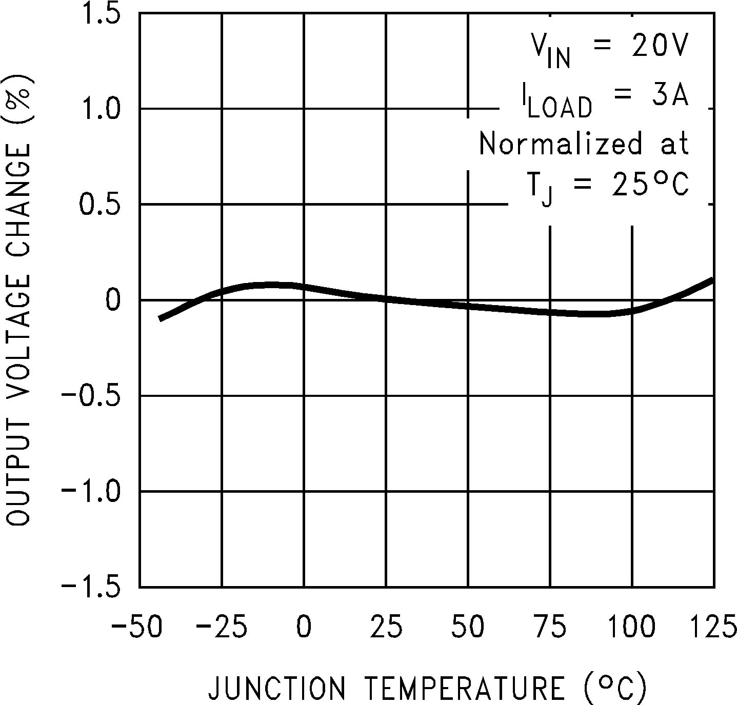 Figure 1. Normalized Output Voltage
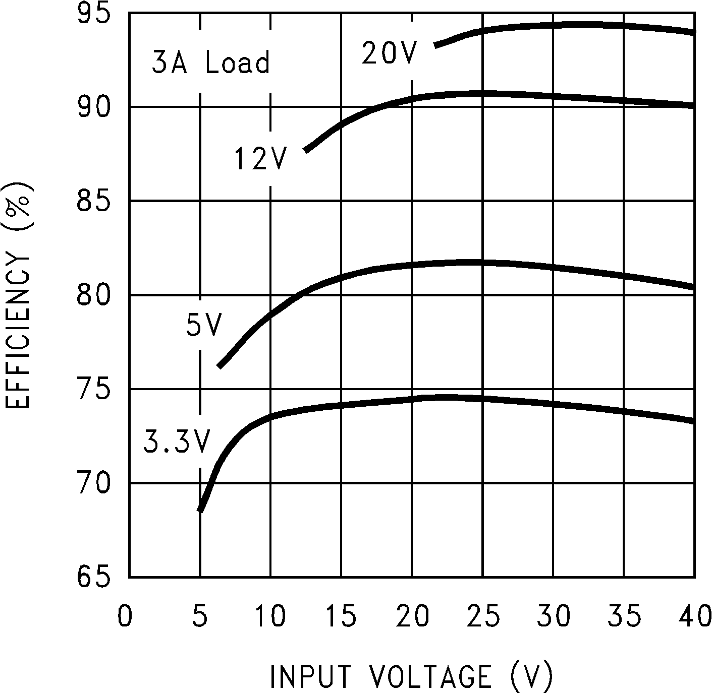 Figure 3. Efficiency
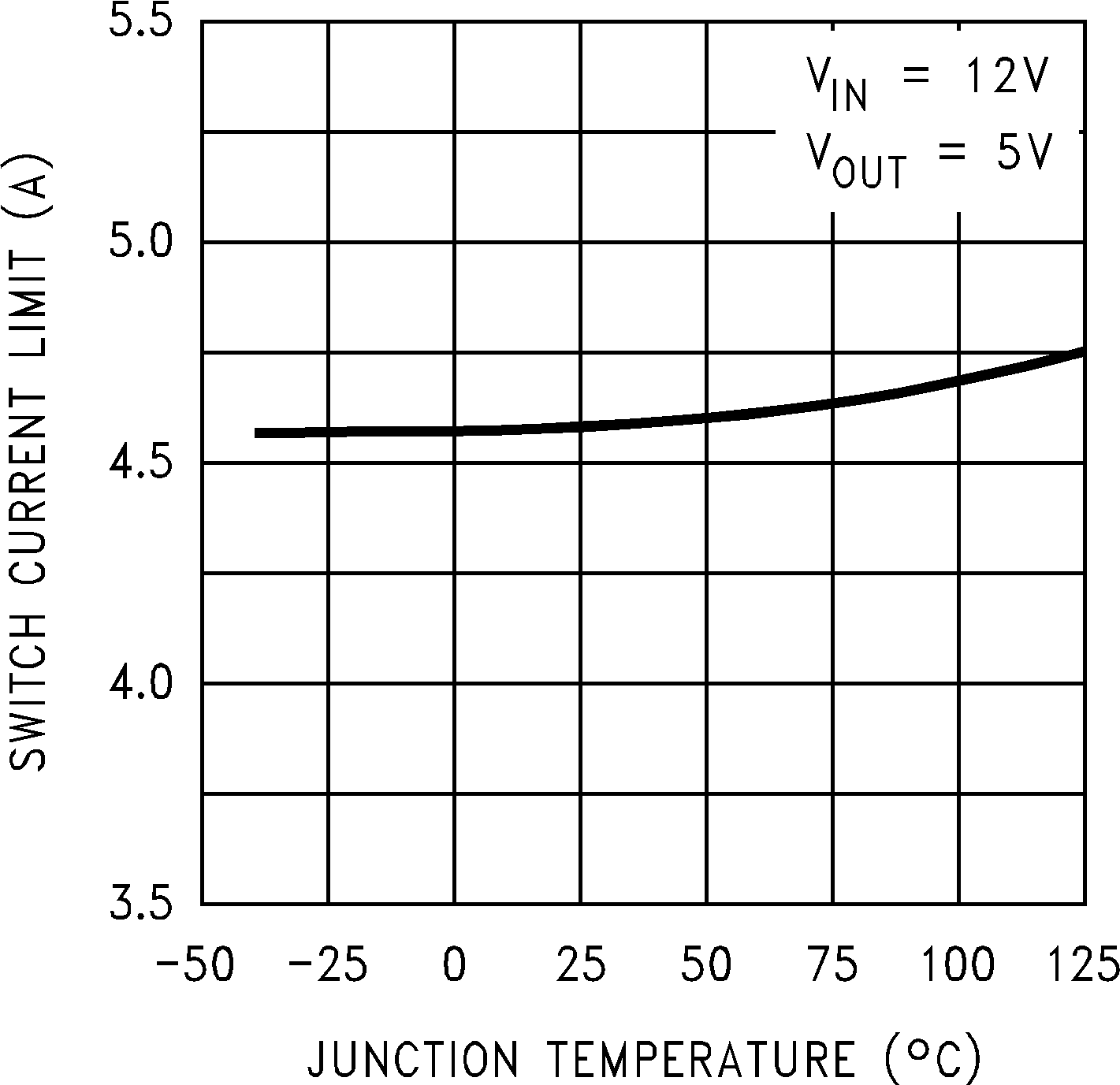 Figure 5. Switch Current Limit
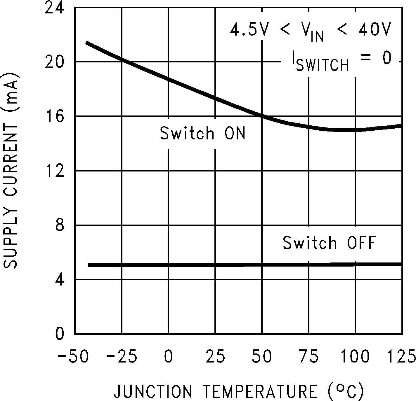 Figure 7. Operating Quiescent Current
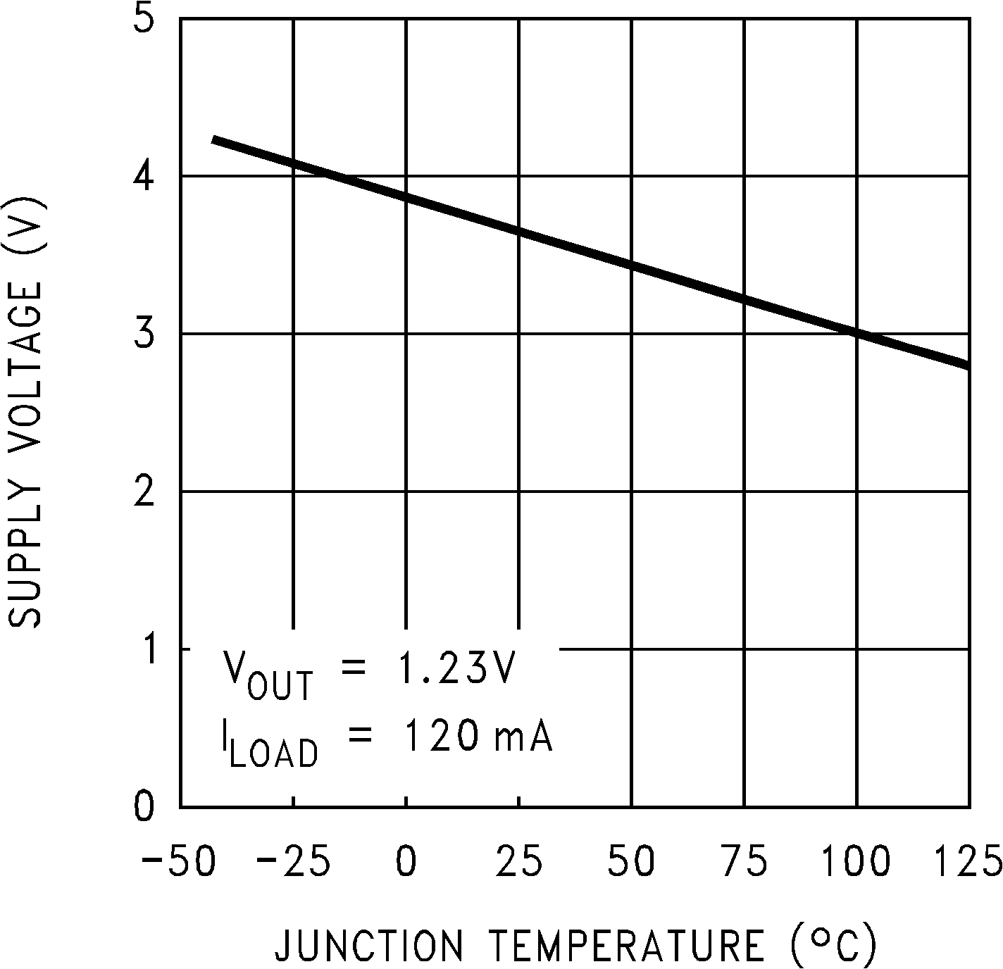 Figure 9. Minimum Operating Supply Voltage
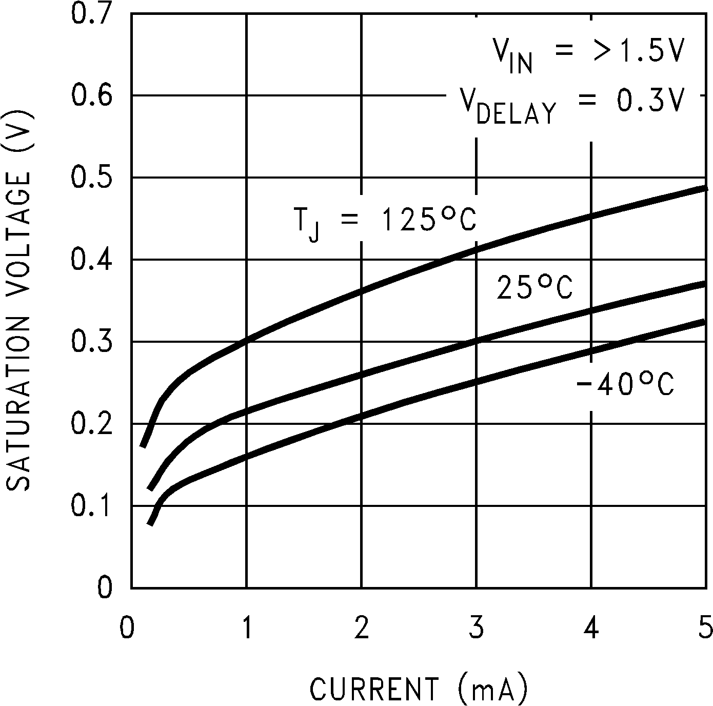 Figure 11. Flag Saturation Voltage
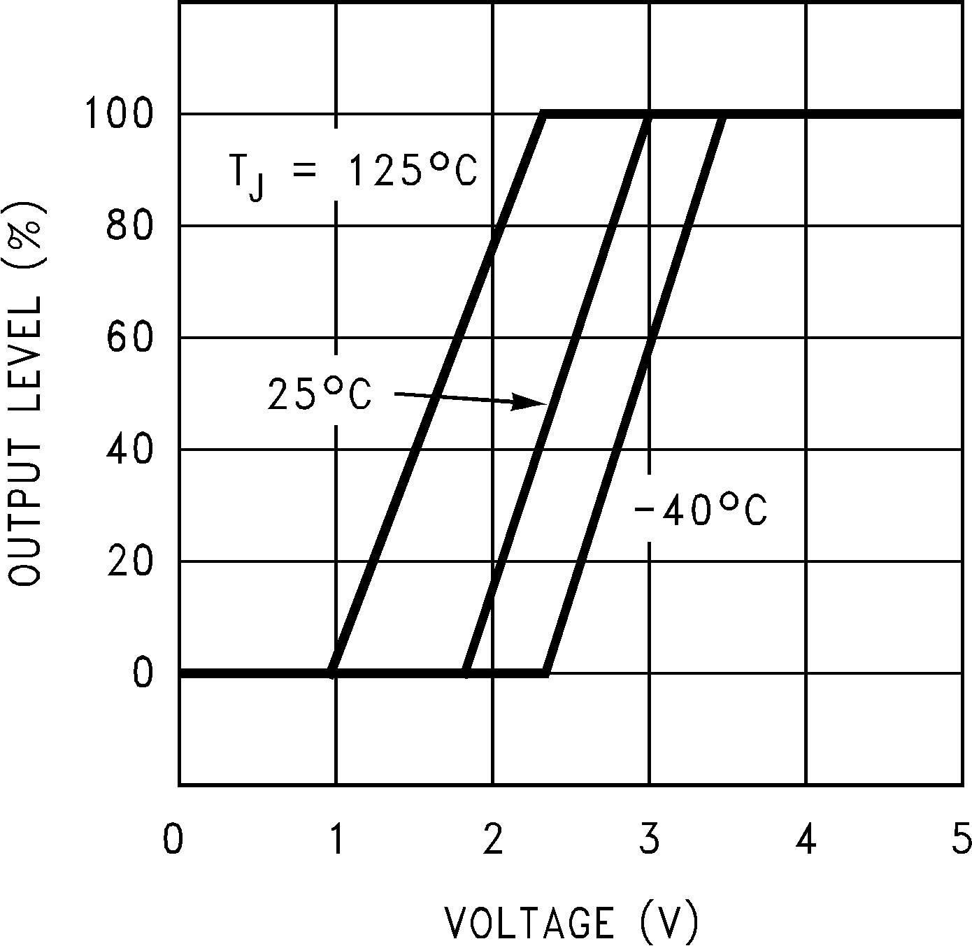 Figure 13. Soft-Start
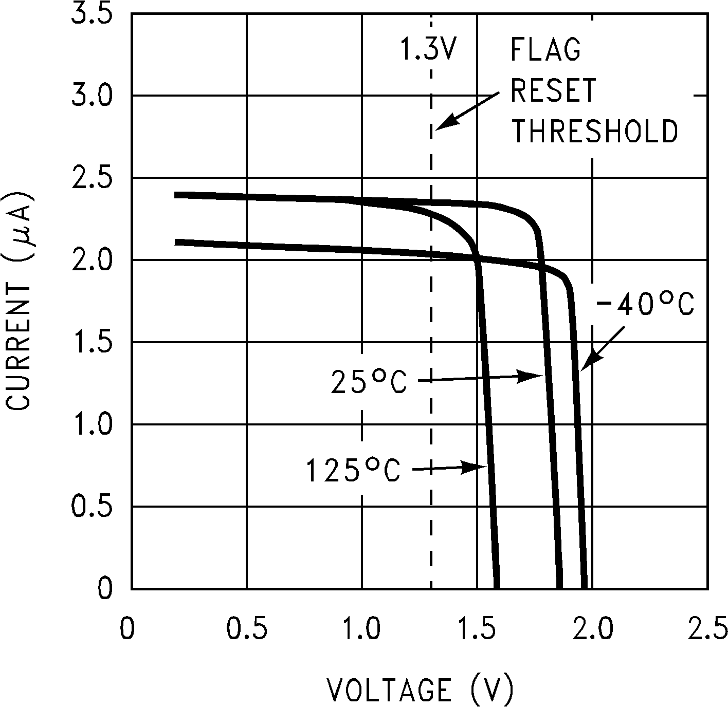 Figure 15. Daisy Pin Current
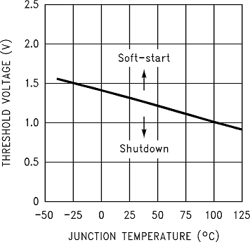 Figure 17. Shutdown/Soft-Start Threshold Voltage
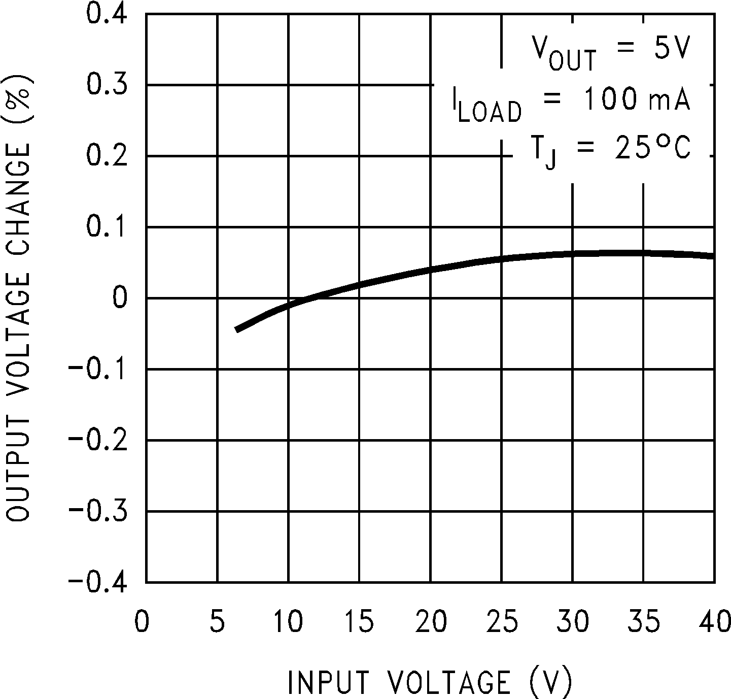 Figure 2. Line Regulation
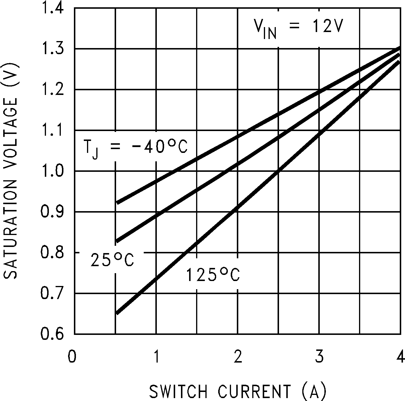 Figure 4. Switch Saturation Voltage
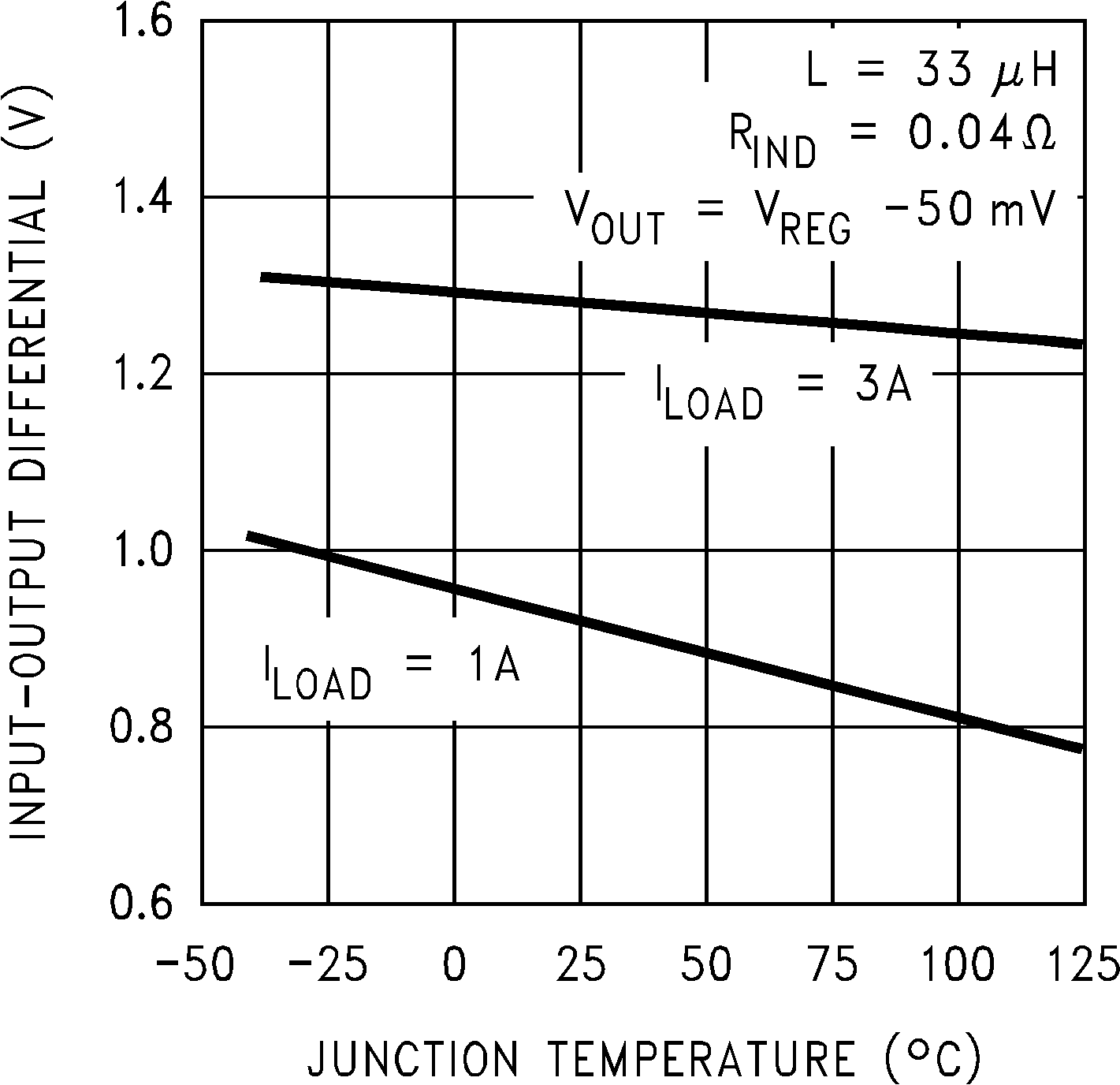 Figure 6. Dropout Voltage
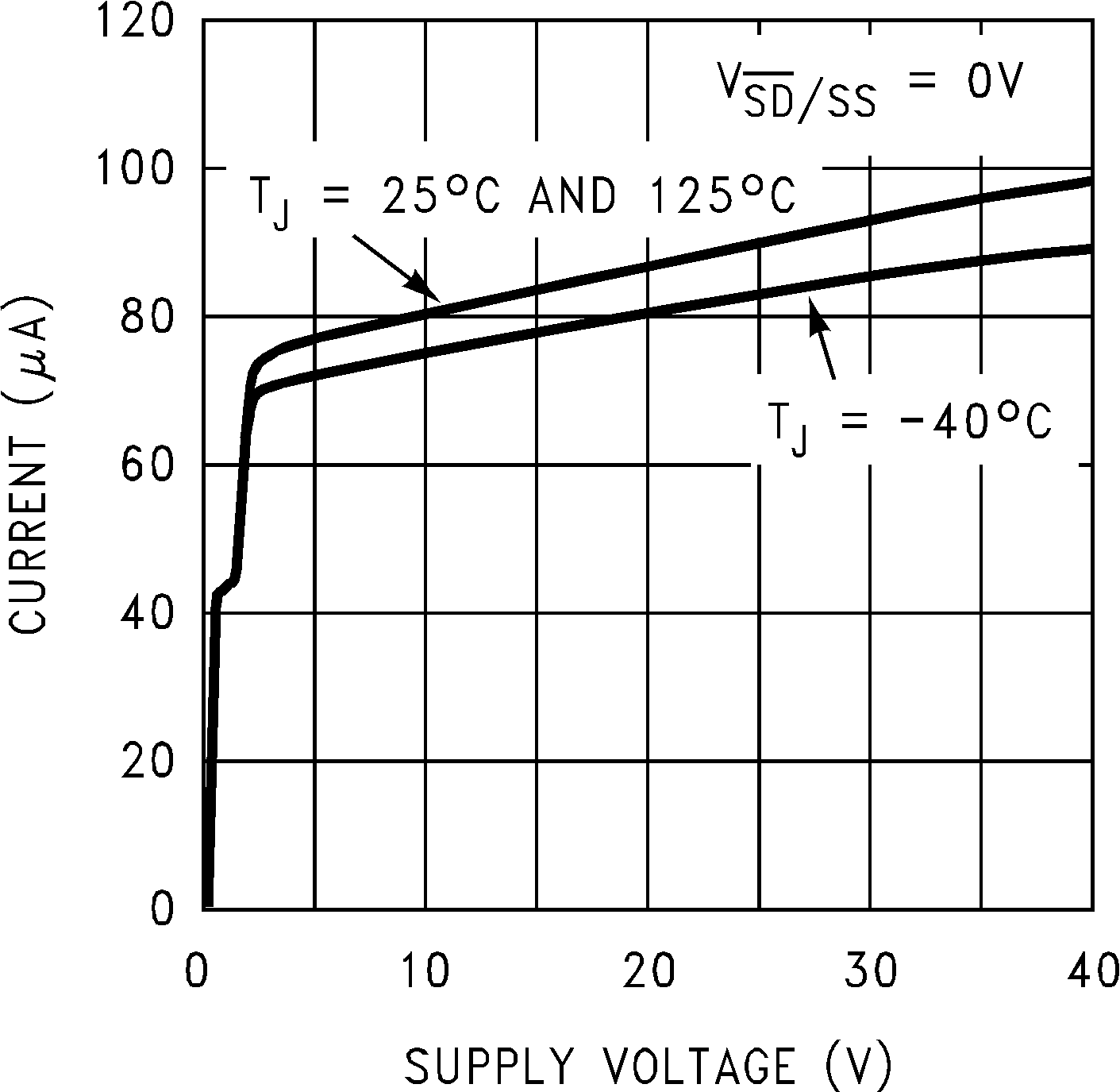 Figure 8. Shutdown Quiescent Current
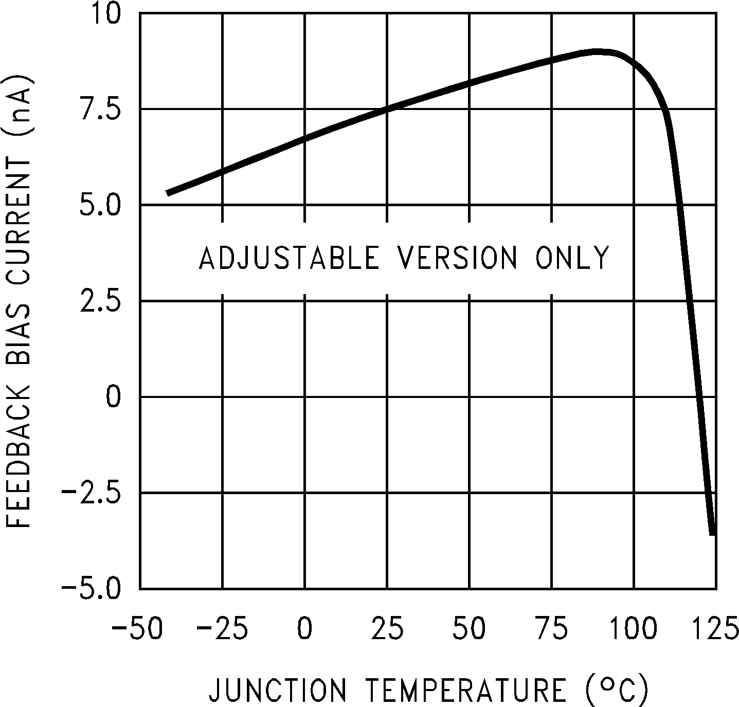 Figure 10. Feedback Pin Bias Current
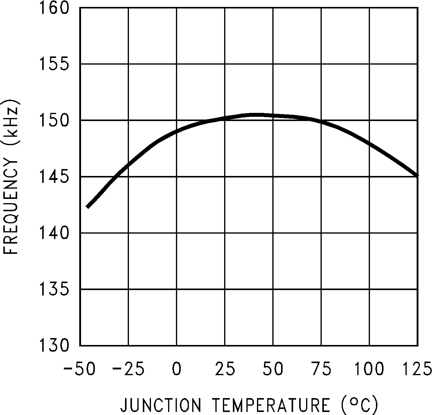 Figure 12. Switching Frequency
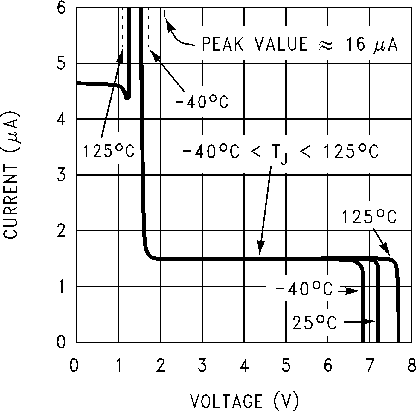 Figure 14. Shutdown/Soft-Start Current
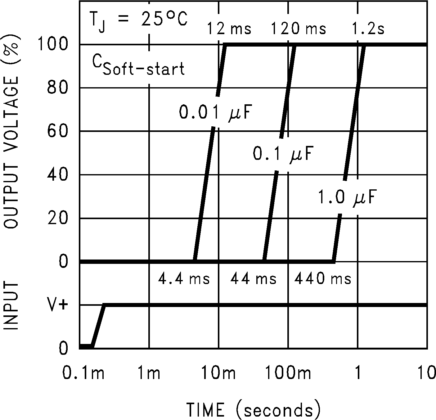 Figure 16. Soft-Start Response
8 Detailed Description
8.1 Overview
The LM2599 SIMPLE SWITCHER® regulator is an easy-to-use, nonsynchronous, step-down DC-DC converter with a wide input voltage range up to 40 V. The regulator is capable of delivering up to 3-A DC load current with excellent line and load regulation. These devices are available in fixed output voltages of 3.3 V, 5 V, 12 V, and an adjustable output version. The family requires few external components, and the pin arrangement was designed for simple, optimum PCB layout.
8.2 Functional Block Diagram

8.3 Feature Description
8.3.1 Shutdown/Soft-Start
The circuit shown in Figure 20 is a standard buck regulator with 20-VIN, 12-VOUT, 1-A load using a 0.068-μF soft-start capacitor. Figure 18 and Figure 19 show the effects of soft-start on the output voltage, the input current, with, and without a soft-start capacitor. The reduced input current required at startup is very evident when comparing the two photos. The soft-start feature reduces the start-up current from 2.6 A down to 650 mA, and delays and slows down the output voltage rise time.
 Figure 18. Output Voltage and Input Current
at Start-Up With Soft-Start
 Figure 19. Output Voltage and Input Current
at Start-Up Without Soft-Start
This reduction in start-up current is useful in situations where the input power source is limited in the amount of current it can deliver. In some applications soft-start can be used to replace undervoltage lockout or delayed start-up functions.
If a very slow output voltage ramp is desired, the soft-start capacitor can be made much larger. Many seconds or even minutes are possible.
If only the shutdown feature is needed, the soft-start capacitor can be eliminated.
 Figure 20. Typical Circuit Using Shutdown/Soft-Start and Error Flag Features
 Figure 21. Inverting −5-V Regulator With Shutdown and Soft-Start
8.3.2 Inverting Regulator
The circuit in Figure 21 converts a positive input voltage to a negative output voltage with a common ground. The circuit operates by bootstrapping the ground pin of the regulator to the negative output voltage, then grounding the feedback pin, the regulator senses the inverted output voltage and regulates it.
This example uses the LM2599-5 to generate a −5-V output, but other output voltages are possible by selecting other output voltage versions, including the adjustable version. Because this regulator topology can produce an output voltage that is either greater than or less than the input voltage, the maximum output current greatly depends on both the input and output voltage. The curve shown in Figure 22 provides a guide as to the amount of output load current possible for the different input and output voltage conditions.
The maximum voltage appearing across the regulator is the absolute sum of the input and output voltage, and this must be limited to a maximum of 40 V. In this example, when converting 20 V to −5 V, the regulator would see 25 V between the input pin and ground pin. The LM2599 has a maximum input voltage rating of 40 V.
 Figure 22. Maximum Load Current for Inverting Regulator Circuit
An additional diode is required in this regulator configuration. Diode D1 is used to isolate input voltage ripple or noise from coupling through the CIN capacitor to the output, under light or no load conditions. Also, this diode isolation changes the topology to closely resemble a buck configuration, thus providing good closed-loop stability. TI recommends a Schottky diode for low input voltages, (because of its lower voltage drop) but for higher input voltages, a IN5400 diode could be used.
Because of differences in the operation of the inverting regulator, the standard design procedure is not used to select the inductor value. In the majority of designs, a 33-μH, 3.5-A inductor is the best choice. Capacitor selection can also be narrowed down to just a few values. Using the values shown in Figure 21 provides good results in the majority of inverting designs.
This type of inverting regulator can require relatively large amounts of input current when starting up, even with light loads. Input currents as high as the LM2599 current limit (approximately 4.5 A) are needed for 2 ms or more, until the output reaches its nominal output voltage. The actual time depends on the output voltage and the size of the output capacitor. Input power sources that are current limited or sources that can not deliver these currents without getting loaded down, may not work correctly. Because of the relatively high startup currents required by the inverting topology, the soft-start feature shown in Figure 21 is recommended.
Also shown in Figure 21 are several shutdown methods for the inverting configuration. With the inverting configuration, some level shifting is required, because the ground pin of the regulator is no longer at ground, but is now at the negative output voltage. The shutdown methods shown accept ground referenced shutdown signals.
8.3.3 Undervoltage Lockout
Some applications require the regulator to remain off until the input voltage reaches a predetermined voltage. Figure 23 contains a undervoltage lockout circuit for a buck configuration, while Figure 24 and Figure 25 are for the inverting types (only the circuitry pertaining to the undervoltage lockout is shown). Figure 23 uses a Zener diode to establish the threshold voltage when the switcher begins operating. When the input voltage is less than the Zener voltage, resistors R1 and R2 hold the shutdown/soft-start pin low, keeping the regulator in the shutdown mode. As the input voltage exceeds the Zener voltage, the Zener conducts, pulling the shutdown/soft-start pin high, allowing the regulator to begin switching. The threshold voltage for the undervoltage lockout feature is approximately 1.5 V greater than the Zener voltage.
 Figure 23. Undervoltage Lockout for a Buck Regulator
Figure 24 and Figure 25 apply the same feature to an inverting circuit. Figure 24 features a constant threshold voltage for turn on and turn off (Zener voltage plus approximately one volt). If hysteresis is needed, the circuit in Figure 25 has a turn ON voltage which is different than the turn OFF voltage. The amount of hysteresis is approximately equal to the value of the output voltage. Because the SD/SS pin has an internal 7-V Zener clamp, R2 is needed to limit the current into this pin to approximately 1 mA when Q1 is on.
 Figure 24. Undervoltage Lockout Without Hysteresis for an Inverting Regulator
 Figure 25. Undervoltage Lockout With Hysteresis for an Inverting Regulator
8.3.4 Negative Voltage Charge Pump
Occasionally a low-current negative voltage is needed for biasing parts of a circuit. A simple method of generating a negative voltage using a charge pump technique and the switching waveform present at the OUT pin, is shown in Figure 26. This unregulated negative voltage is approximately equal to the positive input voltage (minus a few volts), and can supply up to a 600 mA of output current. There is a requirement however, that there be a minimum load of 1.2 A on the regulated positive output for the charge pump to work correctly. Also, resistor R1 is required to limit the charging current of C1 to some value less than the LM2599 current limit (typically
4.5 A).
This method of generating a negative output voltage without an additional inductor can be used with other members of the SIMPLE SWITCHER Family, using either the buck or boost topology.
 Figure 26. Charge Pump for Generating a Low-Current, Negative-Output Voltage
8.4 Device Functional Modes
8.4.1 Discontinuous Mode Operation
The selection guide chooses inductor values suitable for continuous mode operation, but for low current applications or high input voltages, a discontinuous mode design may be a better choice. The design would use an inductor that would be physically smaller, and would need only one half to one third the inductance value needed for a continuous mode design. The peak switch and inductor currents is higher in a discontinuous design, but at these low load currents (1 A and below), the maximum switch current is still less than the switch current limit.
Discontinuous operation can have voltage waveforms that are considerably different than a continuous design. The output pin (switch) waveform can have some damped sinusoidal ringing present (see Figure 44). This ringing is normal for discontinuous operation, and is not caused by feedback loop instabilities. In discontinuous operation, there is a period of time where neither the switch nor the diode are conducting, and the inductor current has dropped to zero. During this time, a small amount of energy can circulate between the inductor and the switch and diode parasitic capacitance causing this characteristic ringing. Normally this ringing is not a problem, unless the amplitude becomes great enough to exceed the input voltage, and even then, there is very little energy present to cause damage.
Different inductor types or core materials produce different amounts of this characteristic ringing. Ferrite core inductors have very little core loss and therefore produce the most ringing. The higher core loss of powdered iron inductors produce less ringing. If desired, a series RC could be placed in parallel with the inductor to dampen the ringing.
 Figure 27. Post Ripple Filter Waveform