SNVS188I May 2004 – October 2017 LM2623
PRODUCTION DATA.
- 1 Features
- 2 Applications
- 3 Description
- 4 Revision History
- 5 Pin Configuration And Functions
- 6 Specifications
- 7 Detailed Description
- 8 Applications And Implementation
- 9 Power Supply Recommendations
- 10Layout
- 11Device And Documentation Support
- 12Mechanical, Packaging, And Orderable Information
Package Options
Mechanical Data (Package|Pins)
Thermal pad, mechanical data (Package|Pins)
Orderable Information
8 Applications And Implementation
NOTE
Information in the following applications sections is not part of the TI component specification, and TI does not warrant its accuracy or completeness. TI’s customers are responsible for determining suitability of components for their purposes. Customers should validate and test their design implementation to confirm system functionality.
8.1 Application Information
The LM2623 features a shutdown mode, entry into the shutdown mode is controlled by the active-low logic input pin EN (pin 2). When the logic input to this pin is pulled below 0.15 VDD, the device goes into shutdown mode. The logic input to this pin should be above 0.7 VDD for the device to work in normal start-up mode.
8.2 Typical Application
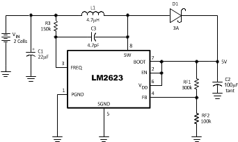
 Figure 9. LM2623 Typical Application
8.2.1 Design Requirements
The LM2623 allows the designer to vary output voltage, operating frequency and duty cycle to optimize the part performance, please read Detailed Design Procedure for details.
8.2.2 Detailed Design Procedure
8.2.2.1 Non-Linear Effect
The LM2623 is very similar to the LM2621. The LM2623 is based on the LM2621, except for the fact that the LM2623 takes advantage of a non-linear effect that allows for the duty cycle to be programmable. The C3 capacitor is used to dump charge on the FREQ pin in order to manipulate the duty cycle of the internal oscillator. The part is being tricked to behave in a certain manner, in the effort to make this Pulse Frequency Modulated (PFM) boost switching regulator behave as a Pulse Width Modulated (PWM) boost switching regulator.
8.2.2.2 Choosing The Correct C3 Capacitor
The C3 capacitor allows for the duty cycle of the internal oscillator to be programmable. Choosing the correct C3 capacitor to get the appropriate duty cycle for a particular application circuit is a trial and error process. The non-linear effect that C3 produces is dependent on the input voltage and output voltage values. The correct C3 capacitor for particular input and output voltage values cannot be calculated. Choosing the correct C3 capacitance is best done by trial and error, in conjunction with the checking of the inductor peak current to make sure your not too close to the current limit of the device. As the C3 capacitor value increases, so does the duty cycle. And conversely as the C3 capacitor value decreases, the duty cycle decreases. An incorrect choice of the C3 capacitor can result in the part prematurely tripping the current limit and/or double pulsing, which could lead to the output voltage not being stable.
8.2.2.3 Setting The Output Voltage
The output voltage of the step-up regulator can be set by connecting a feedback resistive divider made of RF1 and RF2. The resistor values are selected as follows:
A value of 50k to 100k is suggested for RF2. Then, RF1 can be selected using Equation 1.
8.2.2.4 VDD Supply
The VDD supply must be between 3 V to 5 V for the LM2623. This voltage can be bootstrapped from a much lower input voltage by simply connecting the VDD pin to VOUT. In the event that the VDD supply voltage is not a low ripple voltage source (less than 200 millivolts), it may be advisable to use an RC filter to clean it up. Excessive ripple on VDD may reduce the efficiency.
8.2.2.5 Setting The Switching Frequency
The switching frequency of the oscillator is selected by choosing an external resistor (R3) connected between VIN and the FREQ pin. See Figure 3 in the Typical Characteristics section of the data sheet for choosing the R3 value to achieve the desired switching frequency. A high switching frequency allows the use of very small surface mount inductors and capacitors and results in a very small solution size. A switching frequency between 300 kHz and 2 MHz is recommended.
8.2.2.6 Output Diode Selection
A Schottky diode should be used for the output diode. The forward current rating of the diode should be higher than the peak input current, and the reverse voltage rating must be higher than the output voltage. Do not use ordinary rectifier diodes, since slow switching speeds and long recovery times cause the efficiency and the load regulation to suffer.
8.2.3 Application Curves


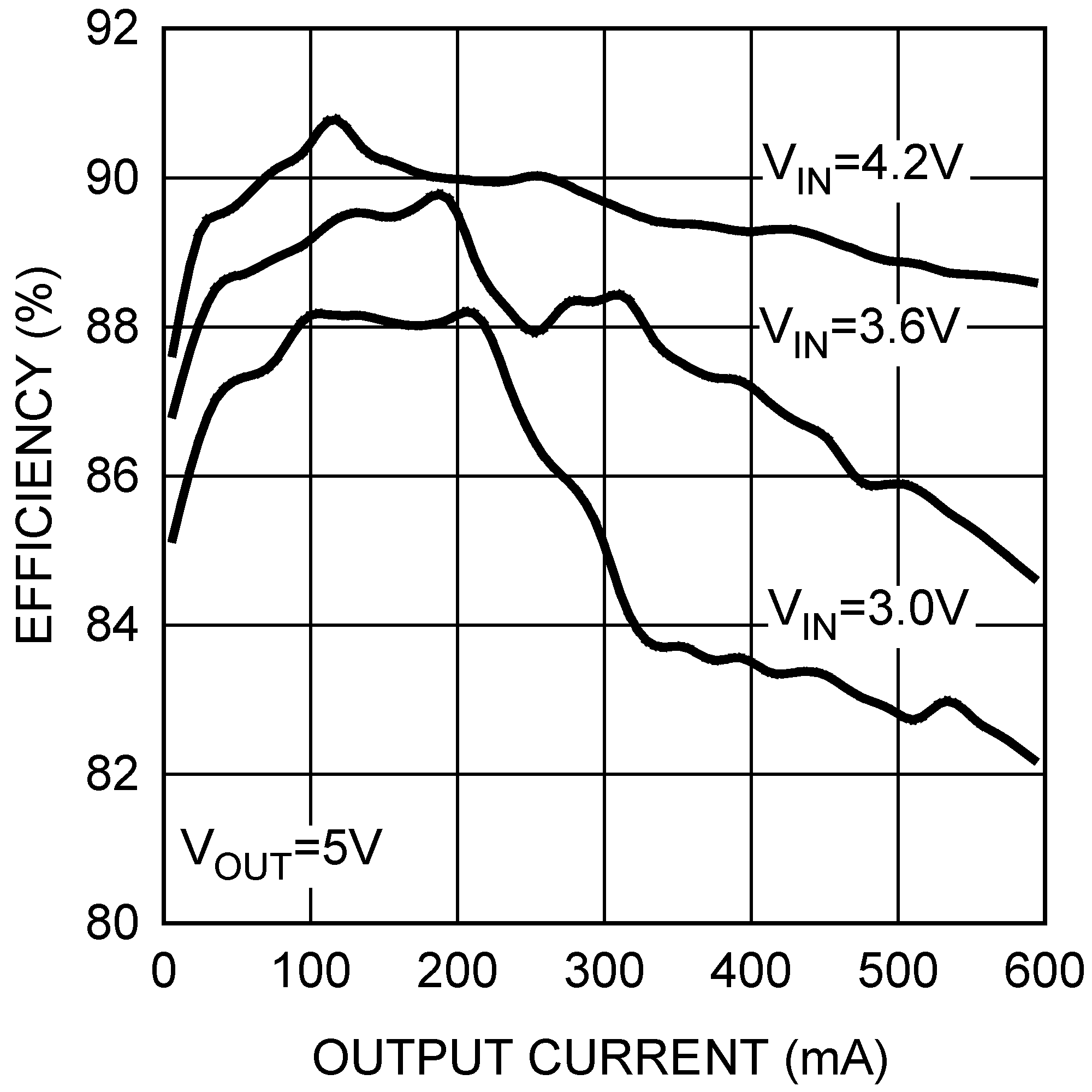
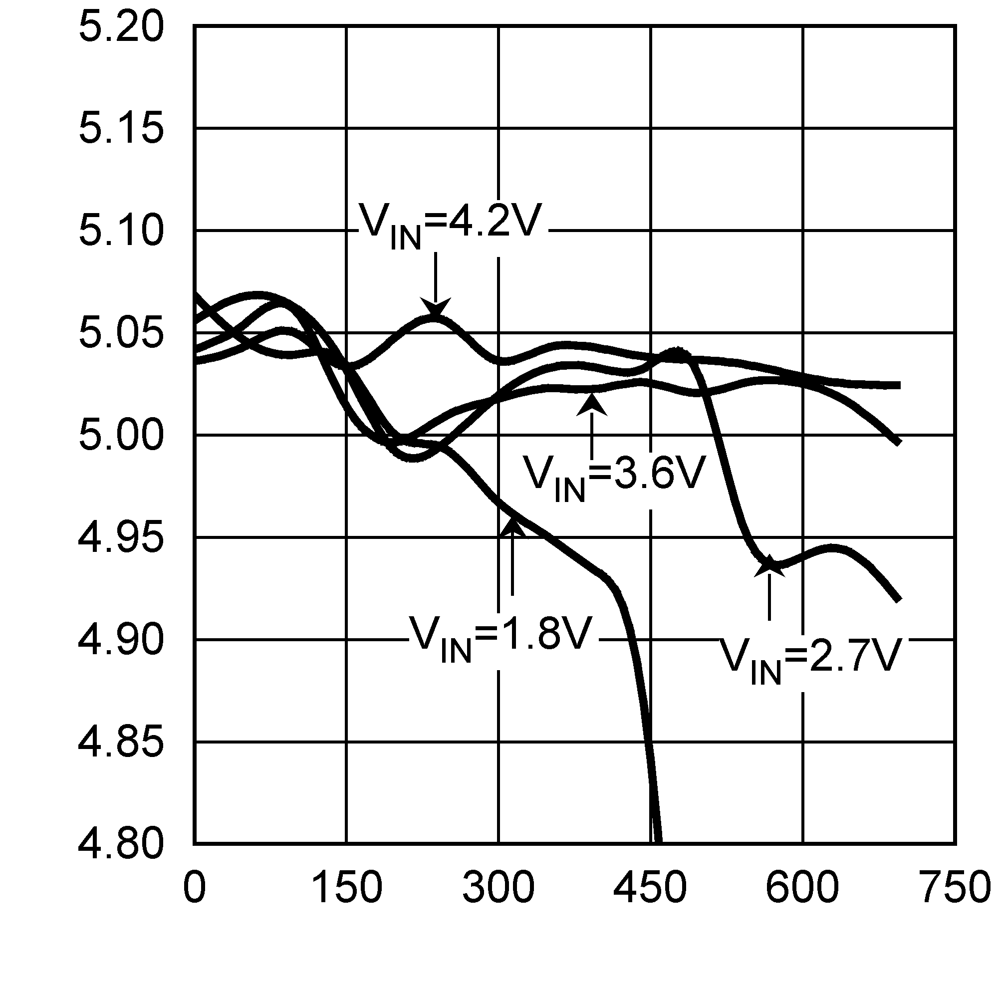
| VOUT = 5 V |