SNVS457D February 2007 – October 2015 LM26400Y
PRODUCTION DATA.
- 1 Features
- 2 Applications
- 3 Description
- 4 Revision History
- 5 Pin Configuration and Functions
- 6 Specifications
- 7 Detailed Description
- 8 Application and Implementation
- 9 Power Supply Recommendations
- 10Layout
- 11Device and Documentation Support
- 12Mechanical, Packaging, and Orderable Information
Package Options
Mechanical Data (Package|Pins)
Thermal pad, mechanical data (Package|Pins)
- PWP|16
Orderable Information
6 Specifications
6.1 Absolute Maximum Ratings
See (1)(2)| MIN | MAX | UNIT | ||
|---|---|---|---|---|
| AVIN, PVIN | –0.5 | 22 | V | |
| SWx Voltage | –0.5 | 22 | V | |
| BSTx Voltage | –0.5 | 26 | V | |
| BSTx to SW Voltage | –0.5 | 6 | V | |
| FBx Voltage | –0.5 | 3 | V | |
| ENx Voltage(3) | –0.5 | 22 | V | |
| SSx Voltage | –0.5 | 3 | V | |
| Junction Temperature | 150 | °C | ||
| Storage Temperature, Tstg | –65 | 150 | °C | |
(1) Stresses beyond those listed under Absolute Maximum Ratings may cause permanent damage to the device. These are stress ratings only, which do not imply functional operation of the device at these or any other conditions beyond those indicated under Recommended Operating Conditions. Exposure to absolute-maximum-rated conditions for extended periods may affect device reliability.
(2) If Military/Aerospace specified devices are required, please contact the Texas Instruments Sales Office/Distributors for availability and specifications.
(3) EN1 and EN2 pins should never be higher than VIN + 0.3 V.
6.2 ESD Ratings
| VALUE | UNIT | |||
|---|---|---|---|---|
| V(ESD) | Electrostatic discharge | Human body model (HBM), per ANSI/ESDA/JEDEC JS-001(1)(2) | ±2000 | V |
(1) JEDEC document JEP155 states that 500-V HBM allows safe manufacturing with a standard ESD control process.
(2) The human body model is a 100-pF capacitor discharged through a 1.5-kΩ resistor into each pin. Test method is per JESD-22-A114.
6.3 Recommended Operating Conditions
over operating free-air temperature range (unless otherwise noted)| MIN | NOM | MAX | UNIT | ||
|---|---|---|---|---|---|
| VIN | 3 | 20 | V | ||
| Junction Temperature | –40 | 125 | °C | ||
6.4 Thermal Information
| THERMAL METRIC(1) | LM26400Y | UNIT | |||
|---|---|---|---|---|---|
| PWP (HTSSOP) | NHQ (WSON) | ||||
| 16 PINS | 16 PINS | ||||
| RθJA | Junction-to-ambient thermal resistance(2)(3) | 39.4 | 27.8 | °C/W | |
| RθJC(top) | Junction-to-case (top) thermal resistance | 24.5 | 27.2 | °C/W | |
| RθJB | Junction-to-board thermal resistance | 18 | 9.9 | °C/W | |
| ψJT | Junction-to-top characterization parameter | 0.7 | 0.3 | °C/W | |
| ψJB | Junction-to-board characterization parameter | 17.8 | 10.1 | °C/W | |
| RθJC(bot) | Junction-to-case (bottom) thermal resistance | 2.1 | 2.8 | °C/W | |
(1) For more information about traditional and new thermal metrics, see the Semiconductor and IC Package Thermal Metrics application report, SPRA953.
(2) Value is highly board-dependent. For comparison of package thermal performance only. Not recommended for prediction of junction temperature in real applications. See Thermal Considerations for more information.
(3) A standard board refers to a four-layer PCB with the size 4.5”x3”x0.063”. Top and bottom copper is 2 oz. Internal plane copper is 1 oz. For details refer to JESD51-7 standard. Mount package on a standard board and test per JESD51-7 standard.
6.5 Electrical Characteristics
Unless otherwise stated, the following conditions apply: AVIN = PVIN = VIN = 5 V. Limits are for TJ = 25°C. Minimum and maximum limits are ensured through test, design, or statistical correlation. Typical values represent the most likely parametric norm at TJ = 25°C, and are provided for reference purposes only.| PARAMETER | TEST CONDITIONS | MIN | TYP | MAX | UNIT | ||
|---|---|---|---|---|---|---|---|
| VFB | Voltages at FB1 and FB2 Pins | Feedback Loop Closed | TJ = 25°C | 0.6 | V | ||
| TJ = 0°C to 85°C | 0.591 | 0.611 | |||||
| Feedback Loop V Closed | TJ = 25°C | 0.6 | |||||
| TJ = –40°C to 125°C | 0.585 | 0.617 | |||||
| ΔVFB_Line | Line Regulation of FB1 and FB2 Voltages, Expressed as PPM Change Per Volt of VIN Variation | VIN = 3 V to 20 V | 66 | ppm/V | |||
| IFB | Current in FB1 and FB2 Pins | VFB = 0.6 V | TJ = 25°C | 0.4 | nA | ||
| TJ = –40°C to 125°C | 250 | ||||||
| VUVLO | Undervoltage Lockout Threshold | VIN Rising From 0 V | TJ = 25°C | 2.7 | V | ||
| TJ = –40°C to 125°C | 2.9 | ||||||
| VIN Falling From 3.3 V | TJ = 25°C | 2.3 | |||||
| TJ = –40°C to 125°C | 2 | ||||||
| VUVLO_HYS | UVLO Hysteresis | TJ = 25°C | 0.36 | V | |||
| TJ = –40°C to 125°C | 0.2 | 0.55 | |||||
| FSW | Switching Frequency | TJ = 25°C | 0.52 | MHz | |||
| TJ = –40°C to 125°C | 0.39 | 0.65 | |||||
| DMAX | Maximum Duty Cycle | TJ = 25°C | 96% | ||||
| TJ = –40°C to 125°C | 90% | ||||||
| DMIN | Minimum Duty Cycle | 2% | |||||
| RDS(ON) | ON-Resistance of Internal Power MOSFET | HTSSOP, 2-A Drain Current | TJ = 25°C | 175 | mΩ | ||
| TJ = –40°C to 125°C | 320 | ||||||
| WSON, 2-A Drain Current | TJ = 25°C | 194 | |||||
| TJ = –40°C to 125°C | 350 | ||||||
| ICL | Peak Current Limit of Internal MOSFET | TJ = 25°C | 3 | A | |||
| TJ = –40°C to 125°C | 2.5 | 4.5 | |||||
| ISD | Shutdown Current of AVIN Pin | EN1 = EN2 = 0 V | 2 | nA | |||
| IQ | Quiescent Current of AVIN Pin (both channels are enabled but not switching) | EN1 = EN2 = 5 V, FB1 = FB2 = 0.7 V, TJ = –40°C to 125°C |
4 | mA | |||
| VEN_IH | Input Logic High of EN1 and EN2 Pins | TJ = –40°C to 125°C | 2.5 | V | |||
| VEN_IL | Input Logic Low of EN1 and EN2 Pins | TJ = –40°C to 125°C | 0.4 | V | |||
| IEN | EN1 and EN2 Currents (sink or source) | 5 | nA | ||||
| ISW_LEAK | Switch Leakage Current Measured at SW1 and SW2 Pins | EN1 = EN2 = SWx = 0 | 1 | µA | |||
| ΔΦ | Phase Shift Between SW1 and SW2 Rising Edges | Feedback Loop Closed. Continuous Conduction Mode. | 170 | 180 | 19 | deg | |
| ISS | SSx Pin Current | TJ = 25°C | 16 | µA | |||
| TJ = –40°C to 125°C | 11 | 21 | |||||
| ΔISS | Difference Between SS1 and SS2 Currents | TJ = –40°C to 125°C | 3 | µA | |||
| VFB_F | FB1 and FB2 Frequency Foldback Threshold | 0.35 | V | ||||
| TSD | Thermal Shutdown Threshold | Junction temperature rises. | 165 | °C | |||
| TSD_HYS | Thermal Shutdown Hysteresis | Junction temperature falls from above TSD. | 15 | °C | |||
6.6 Typical Characteristics
Unless otherwise specified or thermal-shutdown related, TA = 25°C for efficiency curves, loop gain plots and waveforms, and TJ = 25°C for all others.
| VOUT = 5 V |
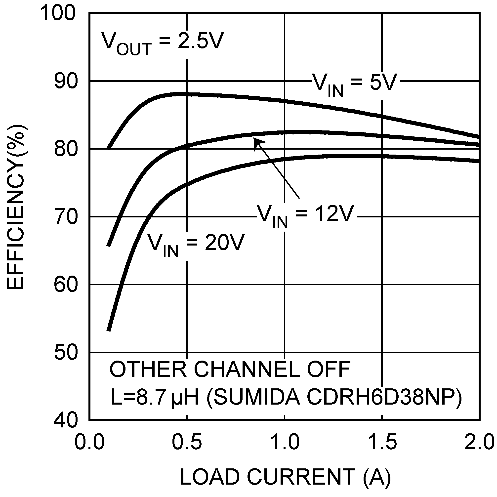
| VOUT = 2.5 V |
 Figure 5. AVIN Shutdown Current vs Temperature
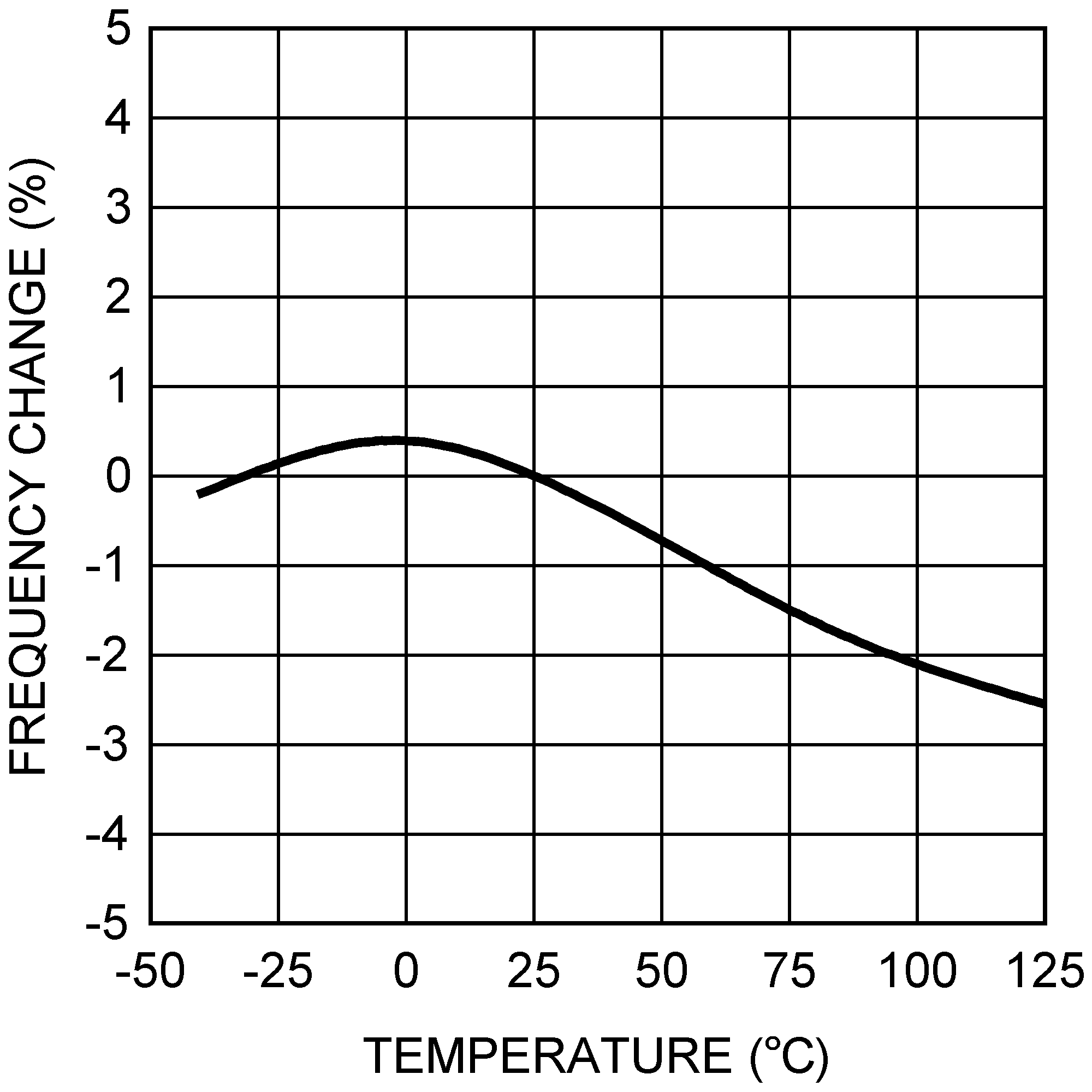 Figure 7. Switching Frequency vs Temperature
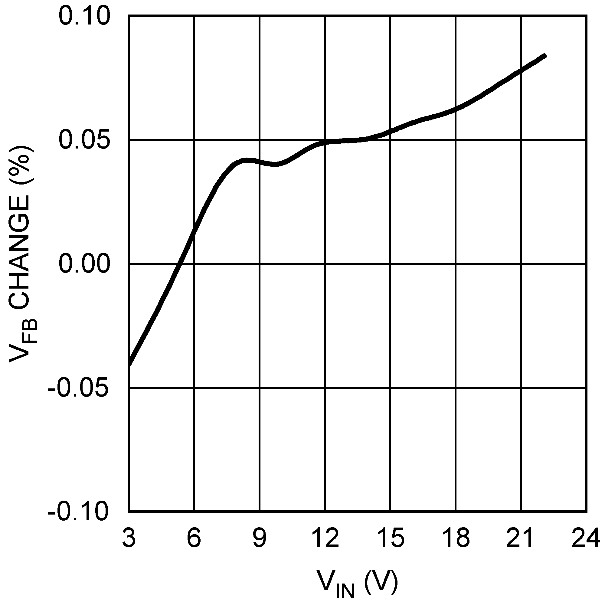 Figure 9. Feedback Voltage vs VIN
 Figure 11. SS-Pin Current vs Temperature
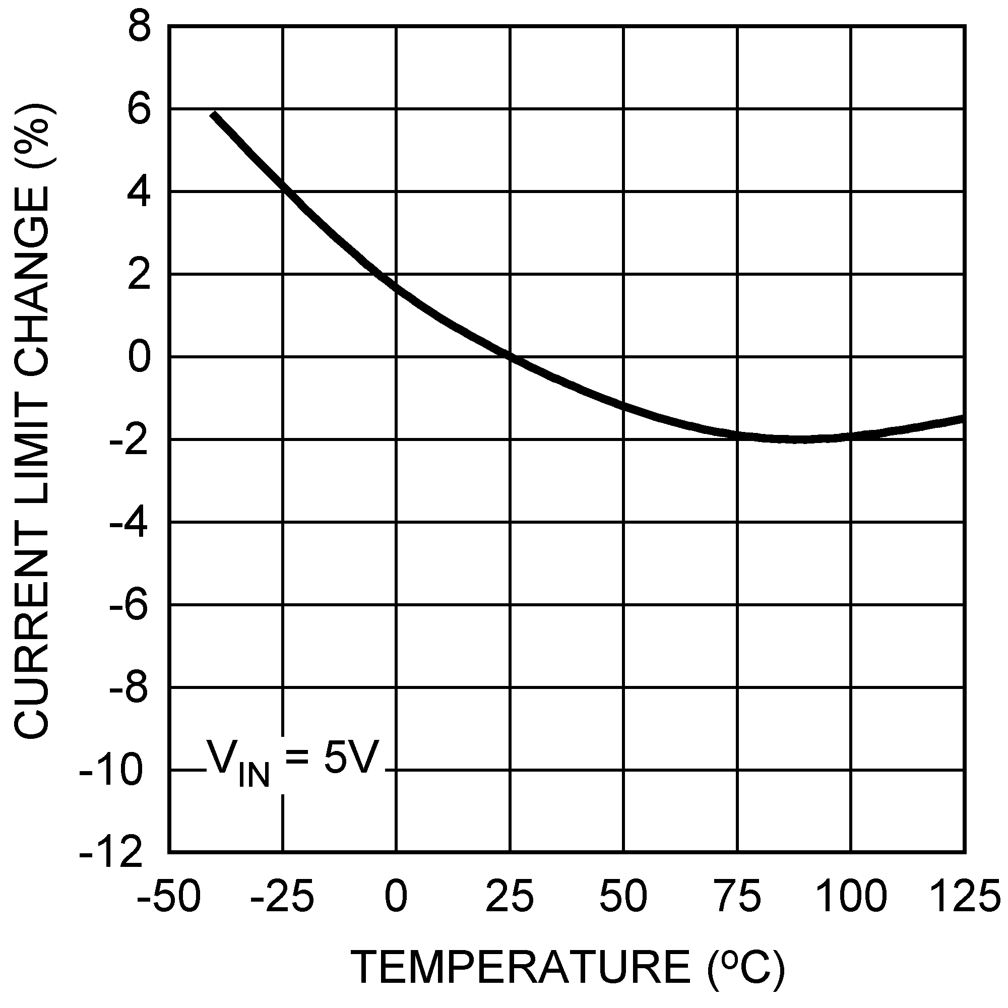 Figure 13. Switch Current Limit vs Temperature
 Figure 15. Loop Gain, DCM

 Figure 19. Shutdown
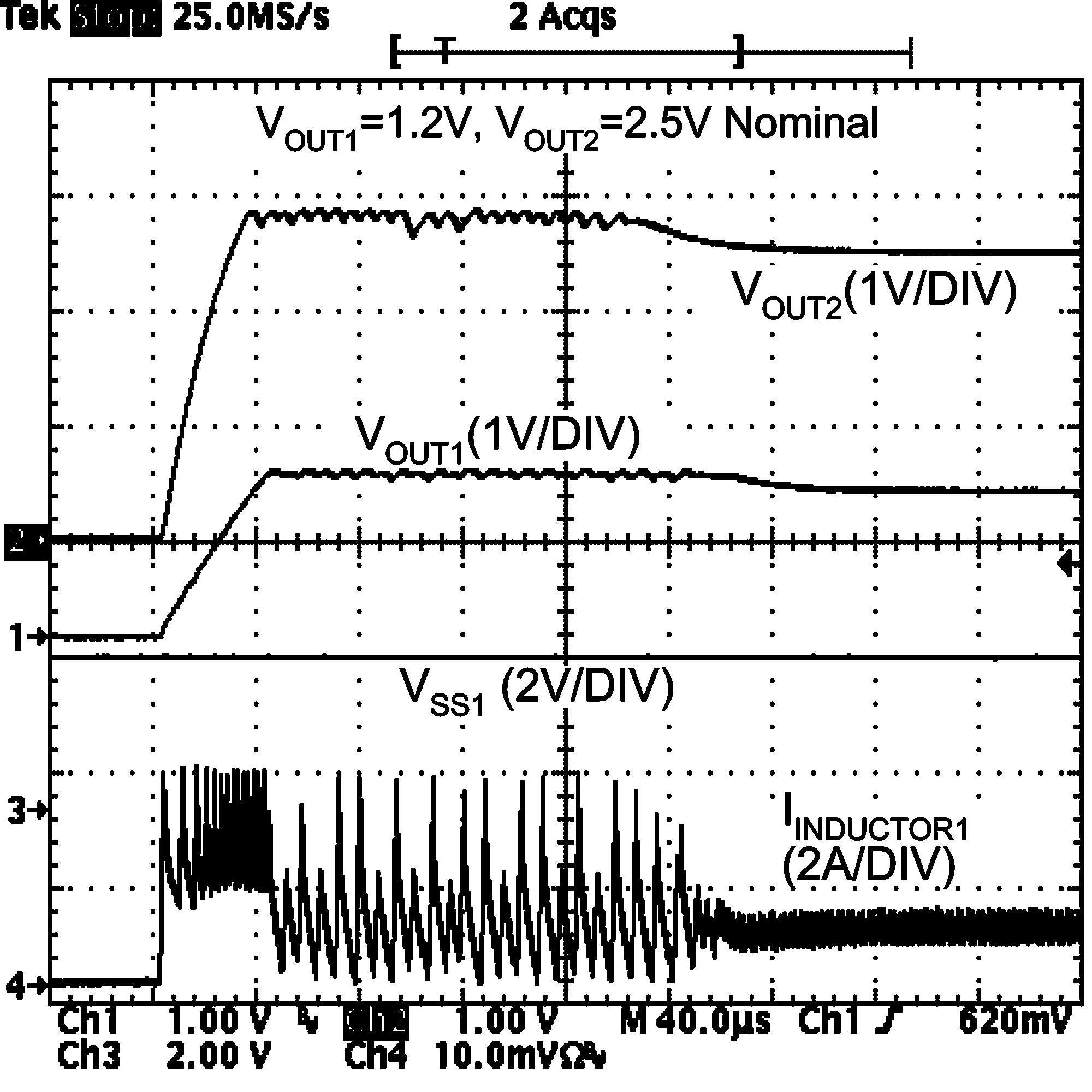 Figure 21. Recovery from Thermal Shutdown
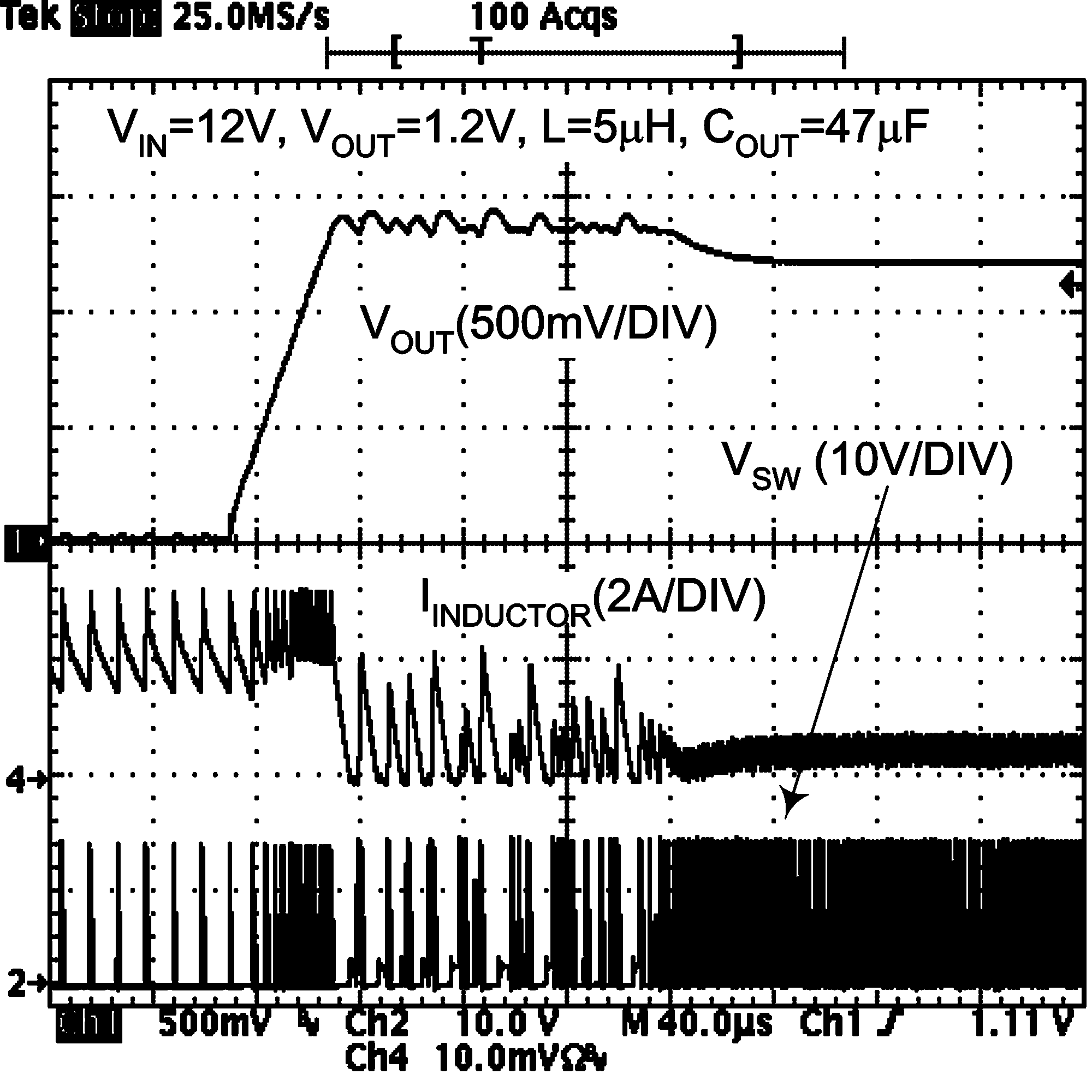 Figure 23. Short-Circuit Release

| VOUT = 3.3 V |

| VOUT = 1.2 V |
 Figure 6. VIN Shutdown Current vs VIN
 Figure 8. Feedback Voltage vs Temperature
 Figure 10. Frequency Foldback
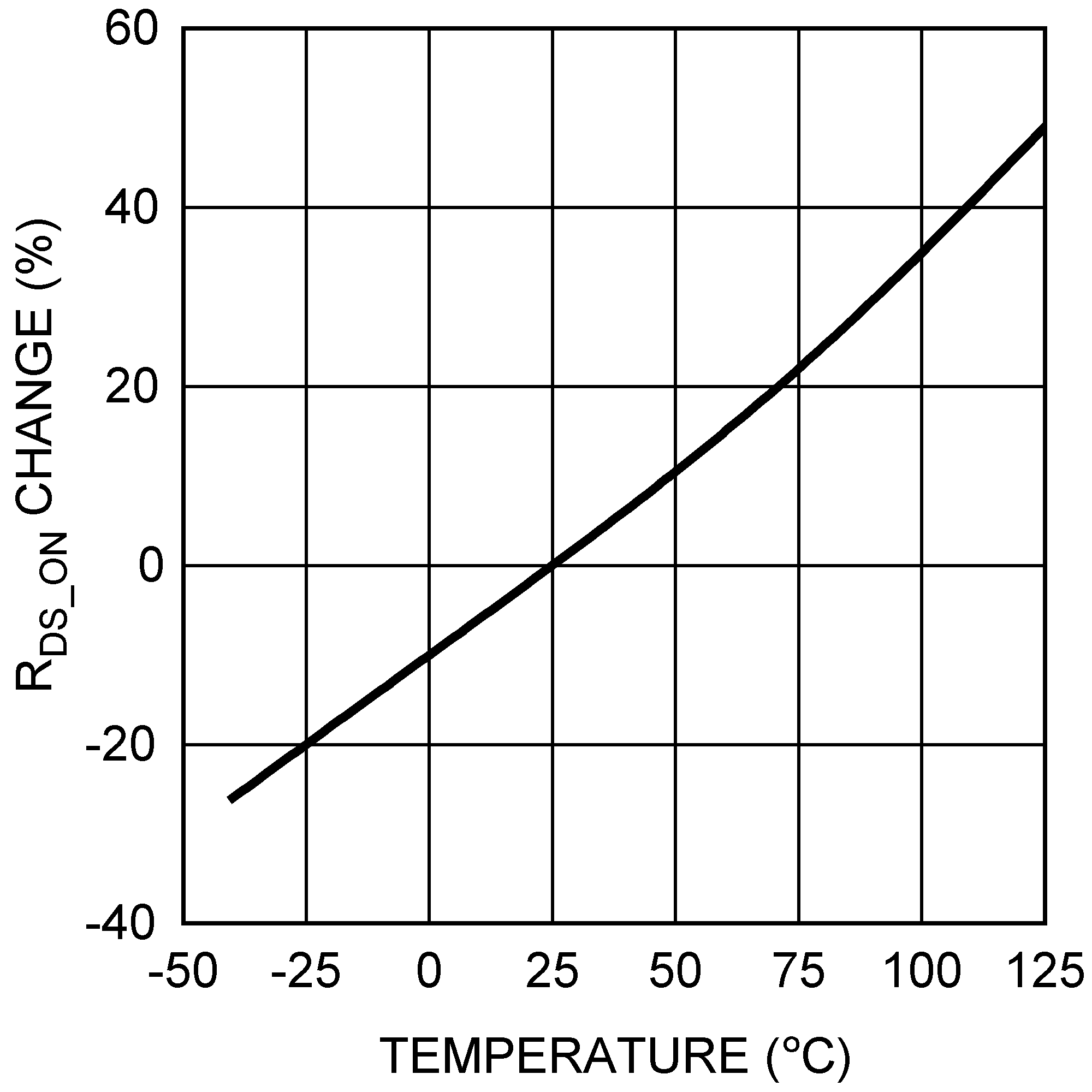 Figure 12. FET RDS_ON vs Temperature

 Figure 16. Loop Gain, CCM
 Figure 18. Line Transient Response
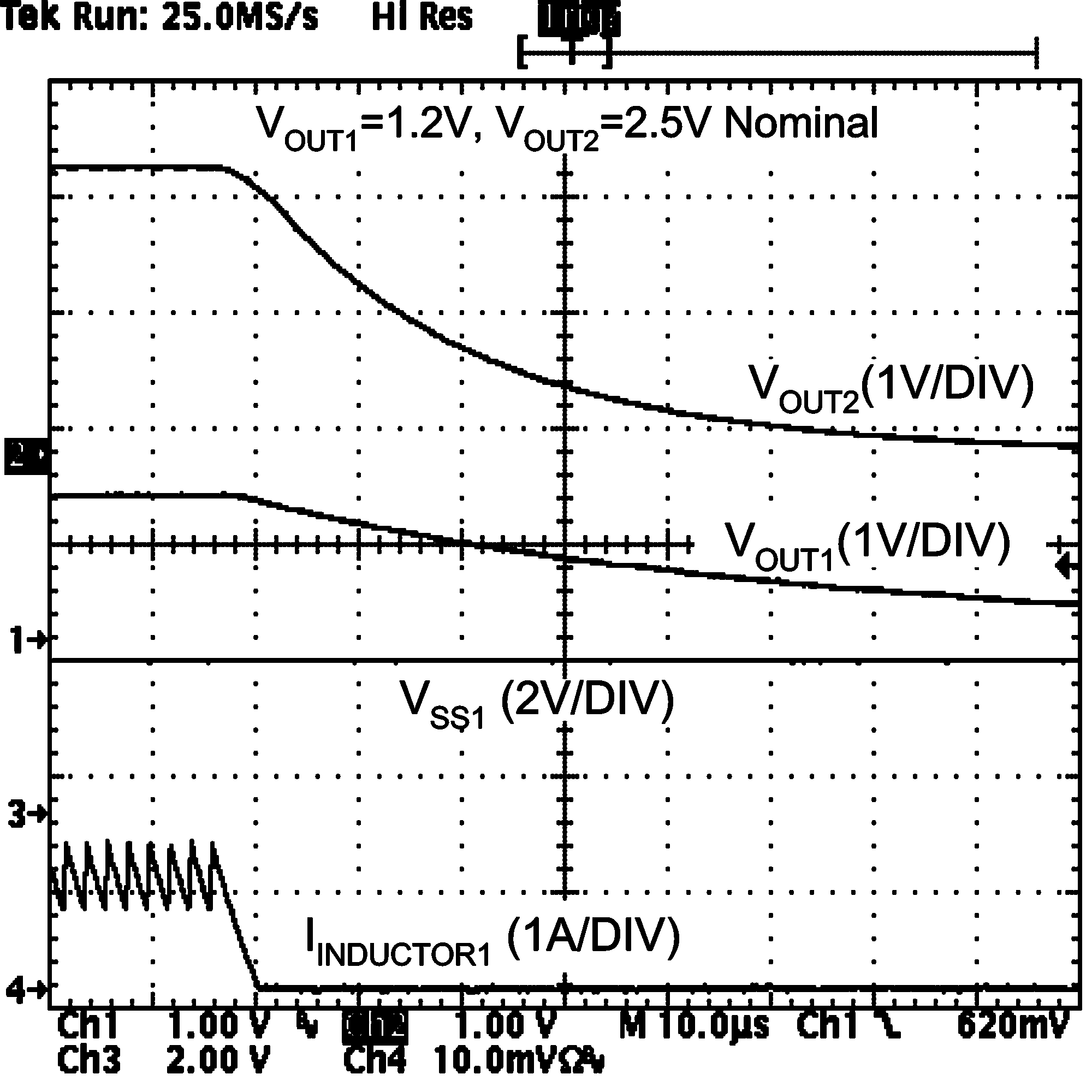 Figure 20. Thermal Shutdown
 Figure 22. Short-Circuit Triggering