SNVSB35C May   2018  – November 2024 LM26420-Q1

PRODUCTION DATA  

  1.   1
  2. Features
  3. Applications
  4. Description
  5. Pin Configuration and Functions
  6. Specifications
    1. 5.1 Absolute Maximum Ratings
    2. 5.2 ESD Ratings
    3. 5.3 Recommended Operating Conditions
    4. 5.4 Thermal Information
    5. 5.5 Electrical Characteristics Per Buck
    6. 5.6 Typical Characteristics
  7. Detailed Description
    1. 6.1 Overview
    2. 6.2 Functional Block Diagram
    3. 6.3 Feature Description
      1. 6.3.1 Soft Start
      2. 6.3.2 Power Good
      3. 6.3.3 Precision Enable
    4. 6.4 Device Functional Modes
      1. 6.4.1 Output Overvoltage Protection
      2. 6.4.2 Undervoltage Lockout
      3. 6.4.3 Current Limit
      4. 6.4.4 Thermal Shutdown
  8. Application and Implementation
    1. 7.1 Application Information
      1. 7.1.1 Programming Output Voltage
      2. 7.1.2 VINC Filtering Components
      3. 7.1.3 Using Precision Enable and Power Good
      4. 7.1.4 Overcurrent Protection for HTSSOP-20 Package
      5. 7.1.5 Current Limit and Short-Circuit Protection for WQFN-16 Package
    2. 7.2 Typical Applications
      1. 7.2.1 2.2-MHz, 0.8-V Typical High-Efficiency Application Circuit
        1. 7.2.1.1 Design Requirements
        2. 7.2.1.2 Detailed Design Procedure
          1. 7.2.1.2.1 Custom Design With WEBENCH® Tools
          2. 7.2.1.2.2 Inductor Selection
          3. 7.2.1.2.3 Input Capacitor Selection
          4. 7.2.1.2.4 Output Capacitor
          5. 7.2.1.2.5 Calculating Efficiency and Junction Temperature
        3. 7.2.1.3 Application Curves
      2. 7.2.2 2.2-MHz, 1.8-V Typical High-Efficiency Application Circuit
        1. 7.2.2.1 Design Requirements
        2. 7.2.2.2 Detailed Design Procedure
        3. 7.2.2.3 Application Curves
      3. 7.2.3 LM26420-Q12.2-MHz, 2.5-V Typical High-Efficiency Application Circuit
        1. 7.2.3.1 Design Requirements
        2. 7.2.3.2 Detailed Design Procedure
        3. 7.2.3.3 Application Curves
    3. 7.3 Power Supply Recommendations
      1. 7.3.1 Power Supply Recommendations - HTSSOP-20 Package
      2. 7.3.2 Power Supply Recommendations - WQFN-16 Package
    4. 7.4 Layout
      1. 7.4.1 Layout Guidelines
      2. 7.4.2 Layout Example
      3. 7.4.3 Thermal Considerations
        1. 7.4.3.1 Method 1: Silicon Junction Temperature Determination
        2. 7.4.3.2 Thermal Shutdown Temperature Determination
  9. Device and Documentation Support
    1. 8.1 Device Support
      1. 8.1.1 Third-Party Products Disclaimer
      2. 8.1.2 Custom Design With WEBENCH® Tools
    2. 8.2 Documentation Support
      1. 8.2.1 Related Documentation
    3. 8.3 Receiving Notification of Documentation Updates
    4. 8.4 Support Resources
    5. 8.5 Trademarks
    6. 8.6 Electrostatic Discharge Caution
    7. 8.7 Glossary
  10. Revision History
  11. 10Mechanical, Packaging, and Orderable Information

Package Options

Mechanical Data (Package|Pins)
Thermal pad, mechanical data (Package|Pins)
Orderable Information

Soft Start

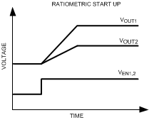
This function forces VOUT to increase at a controlled rate during start-up in a controlled fashion, which helps reduce inrush current and eliminate overshoot on VOUT. During soft start, reference voltage of the error amplifier ramps from 0 V to the nominal value of 0.8 V in approximately 600 µs. If the converter is turned on into a prebiased load, then the feedback begins ramping from the prebias voltage, but at the same rate as if started from 0 V. The two outputs start up ratiometrically if enabled at the same time, see the following figure.
LM26420-Q1 LM26420 Soft StartFigure 6-4 LM26420 Soft Start