SNVSB35C May   2018  – November 2024 LM26420-Q1

PRODUCTION DATA  

  1.   1
  2. Features
  3. Applications
  4. Description
  5. Pin Configuration and Functions
  6. Specifications
    1. 5.1 Absolute Maximum Ratings
    2. 5.2 ESD Ratings
    3. 5.3 Recommended Operating Conditions
    4. 5.4 Thermal Information
    5. 5.5 Electrical Characteristics Per Buck
    6. 5.6 Typical Characteristics
  7. Detailed Description
    1. 6.1 Overview
    2. 6.2 Functional Block Diagram
    3. 6.3 Feature Description
      1. 6.3.1 Soft Start
      2. 6.3.2 Power Good
      3. 6.3.3 Precision Enable
    4. 6.4 Device Functional Modes
      1. 6.4.1 Output Overvoltage Protection
      2. 6.4.2 Undervoltage Lockout
      3. 6.4.3 Current Limit
      4. 6.4.4 Thermal Shutdown
  8. Application and Implementation
    1. 7.1 Application Information
      1. 7.1.1 Programming Output Voltage
      2. 7.1.2 VINC Filtering Components
      3. 7.1.3 Using Precision Enable and Power Good
      4. 7.1.4 Overcurrent Protection for HTSSOP-20 Package
      5. 7.1.5 Current Limit and Short-Circuit Protection for WQFN-16 Package
    2. 7.2 Typical Applications
      1. 7.2.1 2.2-MHz, 0.8-V Typical High-Efficiency Application Circuit
        1. 7.2.1.1 Design Requirements
        2. 7.2.1.2 Detailed Design Procedure
          1. 7.2.1.2.1 Custom Design With WEBENCH® Tools
          2. 7.2.1.2.2 Inductor Selection
          3. 7.2.1.2.3 Input Capacitor Selection
          4. 7.2.1.2.4 Output Capacitor
          5. 7.2.1.2.5 Calculating Efficiency and Junction Temperature
        3. 7.2.1.3 Application Curves
      2. 7.2.2 2.2-MHz, 1.8-V Typical High-Efficiency Application Circuit
        1. 7.2.2.1 Design Requirements
        2. 7.2.2.2 Detailed Design Procedure
        3. 7.2.2.3 Application Curves
      3. 7.2.3 LM26420-Q12.2-MHz, 2.5-V Typical High-Efficiency Application Circuit
        1. 7.2.3.1 Design Requirements
        2. 7.2.3.2 Detailed Design Procedure
        3. 7.2.3.3 Application Curves
    3. 7.3 Power Supply Recommendations
      1. 7.3.1 Power Supply Recommendations - HTSSOP-20 Package
      2. 7.3.2 Power Supply Recommendations - WQFN-16 Package
    4. 7.4 Layout
      1. 7.4.1 Layout Guidelines
      2. 7.4.2 Layout Example
      3. 7.4.3 Thermal Considerations
        1. 7.4.3.1 Method 1: Silicon Junction Temperature Determination
        2. 7.4.3.2 Thermal Shutdown Temperature Determination
  9. Device and Documentation Support
    1. 8.1 Device Support
      1. 8.1.1 Third-Party Products Disclaimer
      2. 8.1.2 Custom Design With WEBENCH® Tools
    2. 8.2 Documentation Support
      1. 8.2.1 Related Documentation
    3. 8.3 Receiving Notification of Documentation Updates
    4. 8.4 Support Resources
    5. 8.5 Trademarks
    6. 8.6 Electrostatic Discharge Caution
    7. 8.7 Glossary
  10. Revision History
  11. 10Mechanical, Packaging, and Orderable Information

Package Options

Mechanical Data (Package|Pins)
Thermal pad, mechanical data (Package|Pins)
Orderable Information

Programming Output Voltage

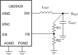
The output voltage is set using Equation 1 where R2 is connected between the FB pin and GND, and R1 is connected between VOUT and the FB pin. A good value for R2 is 10 kΩ. When designing a unity gain converter (VOUT = 0.8 V), R1 must be between 0 Ω and 100 Ω, and R2 must be on the order of 5 kΩ to 50 kΩ. 10 kΩ is the suggested value where R1 is the top feedback resistor and R2 is the bottom feedback resistor.

Equation 1. LM26420-Q1
Equation 2. VREF = 0.80 V
LM26420-Q1 Programming VOUTFigure 7-1 Programming VOUT

To determine the maximum allowed resistor tolerance, use Equation 3:

Equation 3. LM26420-Q1

where

  • TOL is the set point accuracy of the regulator, is the tolerance of VFB.

Example:

VOUT = 2.5 V, with a setpoint accuracy of ±3.5%

Equation 4. LM26420-Q1

Choose 1% resistors. If R2 = 10 kΩ, then R1 is 21.25 kΩ.