SNVSB35C May   2018  – November 2024 LM26420-Q1

PRODUCTION DATA  

  1.   1
  2. Features
  3. Applications
  4. Description
  5. Pin Configuration and Functions
  6. Specifications
    1. 5.1 Absolute Maximum Ratings
    2. 5.2 ESD Ratings
    3. 5.3 Recommended Operating Conditions
    4. 5.4 Thermal Information
    5. 5.5 Electrical Characteristics Per Buck
    6. 5.6 Typical Characteristics
  7. Detailed Description
    1. 6.1 Overview
    2. 6.2 Functional Block Diagram
    3. 6.3 Feature Description
      1. 6.3.1 Soft Start
      2. 6.3.2 Power Good
      3. 6.3.3 Precision Enable
    4. 6.4 Device Functional Modes
      1. 6.4.1 Output Overvoltage Protection
      2. 6.4.2 Undervoltage Lockout
      3. 6.4.3 Current Limit
      4. 6.4.4 Thermal Shutdown
  8. Application and Implementation
    1. 7.1 Application Information
      1. 7.1.1 Programming Output Voltage
      2. 7.1.2 VINC Filtering Components
      3. 7.1.3 Using Precision Enable and Power Good
      4. 7.1.4 Overcurrent Protection for HTSSOP-20 Package
      5. 7.1.5 Current Limit and Short-Circuit Protection for WQFN-16 Package
    2. 7.2 Typical Applications
      1. 7.2.1 2.2-MHz, 0.8-V Typical High-Efficiency Application Circuit
        1. 7.2.1.1 Design Requirements
        2. 7.2.1.2 Detailed Design Procedure
          1. 7.2.1.2.1 Custom Design With WEBENCH® Tools
          2. 7.2.1.2.2 Inductor Selection
          3. 7.2.1.2.3 Input Capacitor Selection
          4. 7.2.1.2.4 Output Capacitor
          5. 7.2.1.2.5 Calculating Efficiency and Junction Temperature
        3. 7.2.1.3 Application Curves
      2. 7.2.2 2.2-MHz, 1.8-V Typical High-Efficiency Application Circuit
        1. 7.2.2.1 Design Requirements
        2. 7.2.2.2 Detailed Design Procedure
        3. 7.2.2.3 Application Curves
      3. 7.2.3 LM26420-Q12.2-MHz, 2.5-V Typical High-Efficiency Application Circuit
        1. 7.2.3.1 Design Requirements
        2. 7.2.3.2 Detailed Design Procedure
        3. 7.2.3.3 Application Curves
    3. 7.3 Power Supply Recommendations
      1. 7.3.1 Power Supply Recommendations - HTSSOP-20 Package
      2. 7.3.2 Power Supply Recommendations - WQFN-16 Package
    4. 7.4 Layout
      1. 7.4.1 Layout Guidelines
      2. 7.4.2 Layout Example
      3. 7.4.3 Thermal Considerations
        1. 7.4.3.1 Method 1: Silicon Junction Temperature Determination
        2. 7.4.3.2 Thermal Shutdown Temperature Determination
  9. Device and Documentation Support
    1. 8.1 Device Support
      1. 8.1.1 Third-Party Products Disclaimer
      2. 8.1.2 Custom Design With WEBENCH® Tools
    2. 8.2 Documentation Support
      1. 8.2.1 Related Documentation
    3. 8.3 Receiving Notification of Documentation Updates
    4. 8.4 Support Resources
    5. 8.5 Trademarks
    6. 8.6 Electrostatic Discharge Caution
    7. 8.7 Glossary
  10. Revision History
  11. 10Mechanical, Packaging, and Orderable Information

Package Options

Mechanical Data (Package|Pins)
Thermal pad, mechanical data (Package|Pins)
Orderable Information

Power Supply Recommendations - HTSSOP-20 Package

The LM26420-Q1 contains a high-side PMOS FET and a low-side NMOS FET for each channel, as shown in Figure 7-15. The source nodes of the high-side PMOS FETs are connected to VIND1 and VIND2, respectively. VINC is the power source for the high-side and low-side gate drivers. Ideally, VINC is connected to VIND1 and VIND2 by an RC filter as detailed in Section 7.1.2. If VINC is allowed to be lower than VIND1 or VIND2, the high-side PMOS FETs can be turned on regardless of the state of the respective gate drivers. Under this condition, shoot through occurs when the low-side NMOS FET is turned on and permanent damage can result. When applying input voltage to VINC, VIND1, and VIND2, VINC must not be less than VIND1,2 – VTH to avoid shoot through and FET damage.
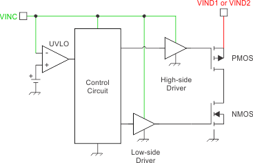
LM26420-Q1 VINC, VIND1,
                        and VIND2 Connection Figure 7-15 VINC, VIND1, and VIND2 Connection