SNVS031M april 2000 – may 2023 LM2676
PRODUCTION DATA
- 1 Features
- 2 Applications
- 3 Description
- 4 Revision History
- 5 Pin Configuration and Functions
-
6 Specifications
- 6.1 Absolute Maximum Ratings
- 6.2 ESD Ratings
- 6.3 Recommended Operating Conditions
- 6.4 Thermal Information
- 6.5 Electrical Characteristics: LM2676 – 3.3 V
- 6.6 Electrical Characteristics: LM2676 – 5 V
- 6.7 Electrical Characteristics: LM2676 – 12 B
- 6.8 Electrical Characteristics: LM2676 – Adjustable
- 6.9 Electrical Characteristics – All Output Voltage Versions
- 6.10 Typical Characteristics
- 7 Detailed Description
- 8 Application and Implementation
- 9 Device and Documentation Support
- 10Mechanical, Packaging, and Orderable Information
Package Options
Mechanical Data (Package|Pins)
Thermal pad, mechanical data (Package|Pins)
- KTW|7
Orderable Information
8.4.1 Layout Guidelines
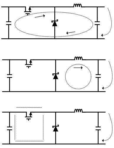
Board layout is critical for the proper operation of switching power supplies. First, the ground plane area must be sufficient for thermal dissipation purposes. Second, appropriate guidelines must be followed to reduce the effects of switching noise. Switch mode converters are very fast switching devices. In such cases, the rapid increase of input current combined with the parasitic trace inductance generates unwanted L di/dt noise spikes. The magnitude of this noise tends to increase as the output current increases. This noise can turn into electromagnetic interference (EMI) and can also cause problems in device performance. Therefore, take care in layout to minimize the effect of this switching noise. The most important layout rule is to keep the AC current loops as small as possible. Figure 8-8 shows the current flow in a buck converter. The top schematic shows a dotted line which represents the current flow during the top switch ON-state. The middle schematic shows the current flow during the top switch OFF-state. The bottom schematic shows the currents referred to as ac currents. These AC currents are the most critical because they are changing in a very short time period. The dotted lines of the bottom schematic are the traces to keep as short and wide as possible. This also yields a small loop area reducing the loop inductance. To avoid functional problems due to layout, review the PCB layout example. Best results are achieved if the placement of the LM2679 device, the bypass capacitor, the Schottky diode, RFBB, RFBT, and the inductor are placed as shown in the example. Note that, in the layout shown, R1 = RFBB and R2 = RFBT. TI also recommends using 2-oz copper boards or heavier to help thermal dissipation and to reduce the parasitic inductances of board traces. See the AN-1229 SIMPLE SWITCHER® PCB Layout Guidelines application report for more information.
 Figure 8-8 Typical Current Flow on a Buck Converter