SNVS153F May 2001 – September 2016 LM2698
PRODUCTION DATA.
- 1 Features
- 2 Applications
- 3 Description
- 4 Revision History
- 5 Pin Configuration and Functions
- 6 Specifications
- 7 Detailed Description
- 8 Application and Implementation
- 9 Power Supply Recommendations
- 10Layout
- 11Device and Documentation Support
- 12Mechanical, Packaging, and Orderable Information
Package Options
Mechanical Data (Package|Pins)
- DGK|8
Thermal pad, mechanical data (Package|Pins)
Orderable Information
8 Application and Implementation
NOTE
Information in the following applications sections is not part of the TI component specification, and TI does not warrant its accuracy or completeness. TI’s customers are responsible for determining suitability of components for their purposes. Customers should validate and test their design implementation to confirm system functionality.
8.1 Application Information
The following sections detail typical applications for this device with Boost and SEPIC converters. The SEPIC converter allows step-up and step-down operation and provides a decoupling of the input voltage to the output voltage through the central capacitor which can help protect the input or output in case of faults. The WEBENCH® Design Tool may be used to generate a complete design. This tool utilizes an iterative design procedure and has access to a comprehensive database of components. This allows the tool to create an optimized design and allows the user to experiment with various design options.
8.2 Typical Applications
8.2.1 1.25-MHz Boost Converter
Figure 16 shows the LM2698 boosting 3.3 V to 10 V at 300 mA.
 Figure 16. 3.3-V to 10-V Boost Converter
8.2.1.1 Design Requirements
The minimum input voltage for this application is 2.5 V. Absolute Maximum switch node voltage is 18 V which limits the maximum output voltage to less than 17 V. For high output voltage applications (>12 V) proper layout is critical to avoid excessive voltage ringing of the switch node and subsequent damage to the part each time the internal switch turns OFF. In general, proper layout is critical for the efficient operation of the converter. The maximum voltage for VIN is 12 V. If the input of the converter exceeds 12 V, VIN must be connected to another rail or to the input through a linear regulator or similar circuit. Level-Shifted SEPIC shows such an example of a step-down voltage circuit for the VIN pin.
8.2.1.2 Detailed Design Procedure
As discussed in Compensation, the RDS(ON) of the internal FET in the LM2698 raises as the input voltage drops below 5 V (see Typical Characteristics). The minimum input voltage for this application is 2.5 V, at which point the RDS(ON) is approximately 200 mΩ. Substituting these values in for Equation 13, it is found that either a 10 µH (1.25-MHz operation) or a 22 µH (600-kHz operation) is necessary for a stable design. The circuit is operated at 1.25 MHz to allow for a smaller inductance. From the Quick Compensator Design equations, RC is calculated as 18.6 kΩ, and a 20-kΩ resistor is used.
8.2.1.2.1 Compensation
This section presents a step-by-step procedure to design the compensation network at pin 1 (VC) of the LM2698. These design methods produce a conservative and stable control loop.
There is a minimum inductance requirement in any current mode converter. This is a function of VOUT, duty cycle, and switching frequency, among other things. Figure 18 plots the recommended inductance range vs duty cycle for VOUT = 12 V. The two lines represent the upper and lower bounds of the recommended inductance range. The simplified compensation procedure that follows assumes that the inductance never drops below the Q = 5 line. Figure 18 is plotted with Equation 13.

where
- RDSON = 0.15
- Se = 0.072 × fS
- Q = 0.5 and 5
Use Q = 5 to calculate the minimum inductance recommended for a stable design. Choosing an inductor between the Q = 0.5 and Q = 5 values provides a good tradeoff between size and stability. Note that as VIN drops less than 5 V, RDS(ON) increases, as shown in Figure 8. The worst case RDS(ON) must be used when choosing the inductance. To view plots for different Vout, multiply the Y axis by a factor of VOUT / 12, or plot Equation 13 for the respective output voltage.
 Figure 17. Minimum Inductance Requirements
 for (a) fS = 600 kHz
 Figure 18. Minimum Inductance Requirements
 for (b) fS = 1.25 MHz
The goal of the compensation network is to provide the best static and dynamic performance while insuring stability over line and load variations. The relationship of stability and performance can be best analyzed by plotting the magnitude and phase of the open loop frequency response in the form of a bode plot. A typical bode plot of the LM2698 open loop frequency response is shown in Figure 19.
 Figure 19. Bode Plot of the LM2698 Frequency Response Using the Typical Application Circuit
Poles are marked with an X, and zeros are marked with a O. The bolded O labeled fRHP is a right-half plane zero. Right half plane zeros act like normal zeros to the magnitude (20 dB / decade slope influence) and like poles to the phase (–90° shift). Three curves are shown. The powerstage curve is the frequency response of the powerstage, which includes the switch, diode, inductor, output capacitor, and load. The compensator curve is the frequency response of the compensator, which is the error amp combined with the compensation network. T is the product of the powerstage and the compensator and is the complete open loop frequency response. The power stage response is fixed by line and load constraints, while the compensator is set by the external compensation network at pin 1. The compensator can be designed in a few simple steps as follows.
8.2.1.2.1.1 Quick Compensator Design
Calculate the quick compensator design using Equation 14 through Equation 19 (where Equation 15 calculates RLOAD(MIN) and Equation 20 calculates ADC).


where
- ROUT = 875 kΩ
Choose CC1 = 4.7 nF


If the output capacitor is of high ESR (0.1 Ω or higher), it may be necessary to use CC2. A rule of thumb is that if 1 / (2πCOUTESR) (Hz) is lower than fS / 2 (Hz), CC2 must be used. Choose CC2 with Equation 21.
where
- ROUT = output impedance of the error amp (875 kΩ)
8.2.1.2.1.2 Improving Transient Response Time
The above compensator design provides a loop gain with high phase margin for a large stability margin. The transient response time of this loop is limited by the lower mid-frequency gain necessary to achieve a high phase margin. If it is desired to increase the transient response time, CC1 may be decreased. Decreasing CC1 by 2x, 4x, and 6x yields increasingly shorter transient response times, however the loop phase margin becomes progressively lower as CC1 is decreased. When optimizing the loop gain for transient response time, it is recommended to keep the phase margin above 40°.
8.2.1.2.1.3 Additional Comments on the Open Loop Frequency Response
The procedure used here to pick the compensation network provides a good starting point. In most cases, these values is sufficient for a stable design. It is always recommended to check the design in a real test setup. This is easy to do with the aid of a dynamic load. Set the high and low load values to your system requirements and switch between the two at about 1kHz. View the output voltage with an oscilloscope using AC coupling, and zoom in enough to see the waveform react to the load change. Use Table 1 to determine if your design is stable. Remember to use worst case conditions (VIN(MIN), ROUT(MIN), ROUT(MAX)).
Table 1. Compensation Troubleshooting Chart
| RESPONSE | CONCLUSION | WHAT TO CHANGE |
|---|---|---|
| Underdamped, weak attenuation | Nearing instability | Make CC1 larger |
| Underdamped, strong attenuation | Stable | Nothing |
| Critically damped | Stable | Nothing |
| Overdamped | Stable | Nothing |
8.2.1.3 Application Curves
 Figure 20. Efficiency Vin = 3.3 V, Vout = 10 V
(With Sumida CDRH6D38-100 Inductor)
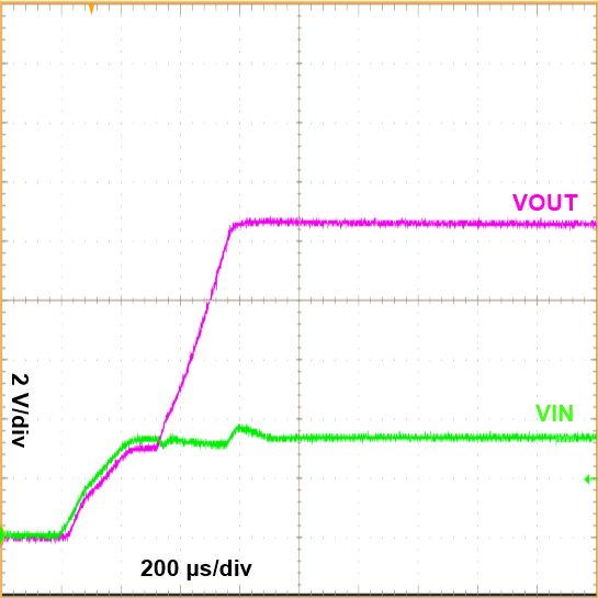
 Figure 21. Start-up Waveform
8.2.2 3.3-V SEPIC
The LM2698 can be used to implement a SEPIC technology. The advantages of the SEPIC topology are that it can step up or step down an input voltage, and it has low input current ripple.
 Figure 22. 3.3-V SEPIC Converter
8.2.2.1 Design Requirements
The input voltage, output voltages, and load currents are necessary to properly design the SEPIC converter. The maximum current that the converter can deliver depends on the internal peak current limit set by the LM2698 and the choice of inductor and switching frequency. See details of the design procedure in the next section. Do not exceed absolute maximum ratings for the pin. The switch node voltage swings between 0 V and VIN+Vout+Vfd, where Vfd is the forward voltage of the diode. In addition to this voltage, the ringing at the switch node could increase the voltage stress on the SW pin and lead to a violation of the absolute maximum voltage on that pin.
8.2.2.2 Detailed Design Procedure
The conversion ratio for the SEPIC is Equation 22.

where
- D' = 1 − D
Solving for D yields Equation 23.

To avoid subharmonic oscillations, it is recommended that inductors L1 and L2 be the same inductance. Currents conducted by the inductors are:
I1 = IOUT(VOUT / VIN)
Δi1 = VIND / (2 × L1 × fs)
I2 = IOUT
Δi1 = VIND / (2 × L2 × fs)
The switch sees a maximum current of I1 + I2 + Δi1 + Δi2. If L1 = L2 = L, the maximum switch current is given by Equation 24.
The maximum load current is limited by this relationship to the switch current.
The polarity of CSEPIC changes between each cycle, so a ceramic capacitor must be used here. A high-quality, low-ESR capacitor directly improves efficiency because all load currents pass through CSEPIC.
CIN must be chosen using the same relationship as in the boost converter. CIN must be able to provide the necessary RMS current.
8.2.2.3 Application Curve
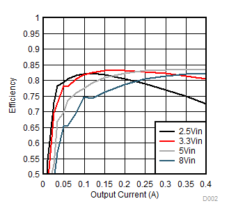
 Figure 23. Efficiency
8.2.3 Level-Shifted SEPIC
The circuit shown in Figure 24 is similar to the SEPIC shown in Figure 22, except that it is level shifted to provide a negative output voltage. This is achieved by connecting the ground of the LM2698 to the output.
 Figure 24. Level-Shifted SEPIC Converter
8.2.3.1 Design Requirements
The circuit analysis for the level-shifted SEPIC is the same as the SEPIC. The voltage at the input of the LM2698 must be clamped if the absolute value of the output voltage plus the input voltage exceeds 12 V, the absolute maximum rating for the VIN pin. The simplest way to do this is with a Zener diode, as shown in Figure 24. Likewise, if the FSLCT pin is pulled high to operate at 1.25 MHz, its voltage must not exceed 12 V. To prevent any high frequency noise from entering the LM2698's internal circuitry, a high-frequency bypass capacitor must be placed as close to pin 6 as possible. A good choice for this capacitor is a 0.1-µF ceramic capacitor.