SNVS153F May 2001 – September 2016 LM2698
PRODUCTION DATA.
- 1 Features
- 2 Applications
- 3 Description
- 4 Revision History
- 5 Pin Configuration and Functions
- 6 Specifications
- 7 Detailed Description
- 8 Application and Implementation
- 9 Power Supply Recommendations
- 10Layout
- 11Device and Documentation Support
- 12Mechanical, Packaging, and Orderable Information
Package Options
Mechanical Data (Package|Pins)
- DGK|8
Thermal pad, mechanical data (Package|Pins)
Orderable Information
6 Specifications
6.1 Absolute Maximum Ratings
over operating free-air temperature range (unless otherwise noted)(1)| MIN | MAX | UNIT | ||
|---|---|---|---|---|
| VIN | –0.3 | 12 | V | |
| SW voltage | –0.3 | 18 | V | |
| FB voltage | –0.3 | 7 | V | |
| VC voltage | 0.965 | 1.565 | V | |
| SHDN voltage(2) | –0.3 | 7 | V | |
| FSLCT(2) | –0.3 | 12 | V | |
| Power dissipation(3) | Internally limited | °C | ||
| Lead temperature | 300 | °C | ||
| Vapor phase temperature (60 s) | 215 | °C | ||
| Infrared temperature (15 s) | 220 | °C | ||
| Junction temperature, TJ | 150 | °C | ||
| Storage temperature, Tstg | –65 | 150 | °C | |
(1) Stresses beyond those listed under Absolute Maximum Ratings may cause permanent damage to the device. These are stress ratings only, which do not imply functional operation of the device at these or any other conditions beyond those indicated under Recommended Operating Conditions. Exposure to absolute-maximum-rated conditions for extended periods may affect device reliability.
(2) Shutdown and voltage frequency select must not exceed VIN.
(3) The maximum allowable power dissipation is a function of the maximum junction temperature, TJ(MAX), the junction-to-ambient thermal resistance, θJA, and the ambient temperature, TA. See the Electrical Characteristics for the thermal resistance of various layouts. The maximum allowable power dissipation at any ambient temperature is calculated using PD (MAX) = (TJ(MAX) – TA) / θJA. Exceeding the maximum allowable power dissipation causes excessive die temperature, and the regulator goes into thermal shutdown.
6.2 ESD Ratings
| VALUE | UNIT | |||
|---|---|---|---|---|
| V(ESD) | Electrostatic discharge | Human-body model (HBM), per ANSI/ESDA/JEDEC JS-001(1) | ±2000 | V |
| Charged-device model (CDM), per JEDEC specification JESD22-C101(2) | ±200 | |||
(1) JEDEC document JEP155 states that 500-V HBM allows safe manufacturing with a standard ESD control process.
(2) JEDEC document JEP157 states that 250-V CDM allows safe manufacturing with a standard ESD control process.
6.3 Recommended Operating Conditions
over operating free-air temperature range (unless otherwise noted)| MIN | NOM | MAX | UNIT | |
|---|---|---|---|---|
| Supply voltage | 2.2 | 12 | V | |
| SW voltage | 0 | 17.5 | V | |
| Operating junction temperature(1) | –40 | 125 | °C |
(1) All limits are specified at room temperature (standard typeface) and at temperature extremes (bold typeface). All room temperature limits are 100% tested or specified through statistical analysis. All limits at temperature extremes are specified via correlation using standard Statistical Quality Control (SQC) methods. All limits are used to calculate Average Outgoing Quality Level (AOQL).
6.4 Thermal Information
| THERMAL METRIC(1) | LM2698 | UNIT | |
|---|---|---|---|
| DGK (VSSOP) | |||
| 8 PINS | |||
| RθJA | Junction-to-ambient thermal resistance | 142.5 | °C/W |
| RθJC(top) | Junction-to-case (top) thermal resistance | 49.7 | °C/W |
| RθJB | Junction-to-board thermal resistance | 69.5 | °C/W |
| ψJT | Junction-to-top characterization parameter | 4 | °C/W |
| ψJB | Junction-to-board characterization parameter | 67.8 | °C/W |
| RθJC(bot) | Junction-to-case (bottom) thermal resistance | — | °C/W |
(1) For more information about traditional and new thermal metrics, see the Semiconductor and IC Package Thermal Metrics application report.
6.5 Electrical Characteristics
TJ = 25°C, VIN =2.2 V, and IL = 0 A (unless otherwise noted)| PARAMETER | TEST CONDITIONS | MIN(1) | TYP(2) | MAX(1) | UNIT | ||
|---|---|---|---|---|---|---|---|
| IQ | Quiescent current | FB = 0 V (not switching) | TJ = 25°C | 1.3 | mA | ||
| TJ = –40°C to 125°C | 2 | ||||||
| VSHDN = 0 V | TJ = 25°C | 5 | µA | ||||
| TJ = –40°C to 125°C | 10 | ||||||
| VFB | Feedback voltage | TJ = 25°C | 1.26 | V | |||
| TJ = –40°C to 125°C | 1.23 | 1.29 | |||||
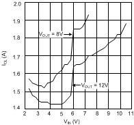
| ICL | Switch current limit | VIN = 2.7 V(3) | TJ = 25°C | 1.9 | A | ||
| TJ = –40°C to 125°C | 1.35 | 2.4 | |||||
| %VFB/ΔVIN | Feedback voltage line regulation | 2.2 V ≤ VIN ≤ 12 V | TJ = 25°C | 0.013% | V | ||
| TJ = –40°C to 125°C | 0.1% | ||||||
| IB | FB pin bias current(4) | TJ = 25°C | 0.5 | nA | |||
| TJ = –40°C to 125°C | 20 | ||||||
| VIN | Input voltage range | TJ = –40°C to 125°C | 2.2 | 12 | V | ||
| gm | Error amp transconductance | ΔI = 5 µA | TJ = 25°C | 135 | µmho | ||
| TJ = –40°C to 125°C | 40 | 290 | |||||
| AV | Error amp voltage gain | 120 | V/V | ||||
| DMAX | Maximum duty cycle | FSLCT = Ground | TJ = 25°C | 85% | |||
| TJ = –40°C to 125°C | 78% | ||||||
| DMIN | Minimum duty cycle | FSLCT = Ground | 15% | ||||
| FSLCT = VIN | 30% | ||||||
| fS | Switching frequency | FSLCT = Ground | TJ = 25°C | 600 | kHz | ||
| TJ = –40°C to 125°C | 480 | 720 | |||||
| FSLCT = VIN | TJ = 25°C | 1.25 | MHz | ||||
| TJ = –40°C to 125°C | 1 | 1.5 | |||||
| ISHDN | Shutdown pin current | VSHDN = VIN | TJ = 25°C | 0.01 | µA | ||
| TJ = –40°C to 125°C | 0.1 | ||||||
| VSHDN = 0 V | TJ = 25°C | –0.5 | |||||
| TJ = –40°C to 125°C | –1 | ||||||
| IL | Switch leakage current | VSW = 18 V | TJ = 25°C | 0.01 | µA | ||
| TJ = –40°C to 125°C | 3 | ||||||
| RDS(ON) | Switch RDS(ON) | VIN = 2.7 V, ISW = 1 A | TJ = 25°C | 0.2 | Ω | ||
| TJ = –40°C to 125°C | 0.4 | ||||||
| THSHDN | SHDN threshold voltage | Output high | TJ = 25°C | 0.6 | V | ||
| TJ = –40°C to 125°C | 0.9 | ||||||
| Output low | TJ = 25°C | 0.6 | |||||
| TJ = –40°C to 125°C | 0.3 | ||||||
| UVP | On threshold | TJ = 25°C | 2.05 | V | |||
| TJ = –40°C to 125°C | 1.95 | 2.2 | |||||
| Off threshold | TJ = 25°C | 1.95 | V | ||||
| TJ = –40°C to 125°C | 1.85 | 2.1 | |||||
(1) All limits are specified at room temperature and at temperature extremes. All room temperature limits are 100% tested or specified through statistical analysis. All limits at temperature extremes are specified via correlation using standard Statistical Quality Control (SQC) methods. All limits are used to calculate Average Outgoing Quality Level (AOQL).
(2) Typical numbers are at 25°C and represent the most likely norm.
(3) This is the switch current limit at 0% duty cycle. The switch current limit changes as a function of duty cycle. See Typical Characteristics for ICL vs VIN.
(4) Bias current flows into FB pin.
6.6 Typical Characteristics
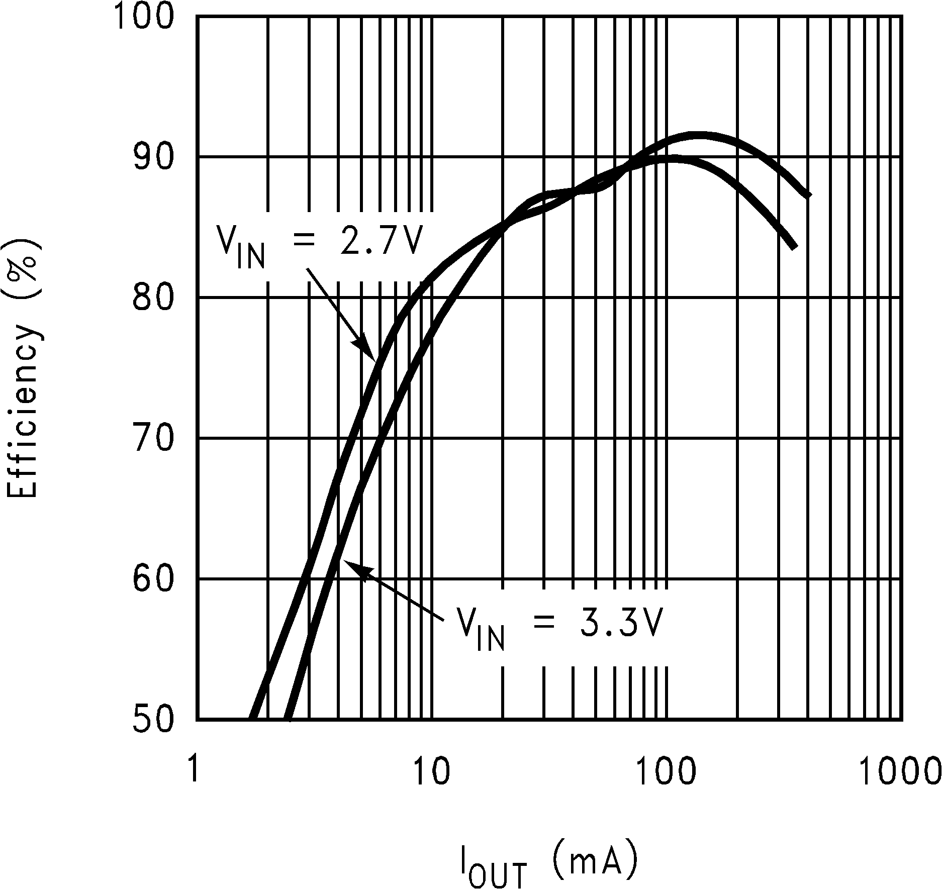
| VOUT = 8 V | fS = 600 kHz |
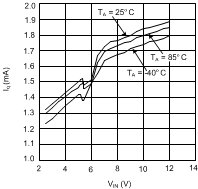
| 600 kHz | Non-Switching |
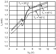
| 1.25 MHz | Non-Switching |
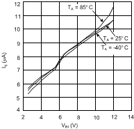 Figure 7. Iq(SHDN) vs VIN
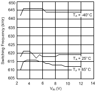 Figure 9. Switching Frequency vs VIN (600 kHz)
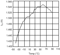
| VIN = 3.3 V | VOUT = 8 V |
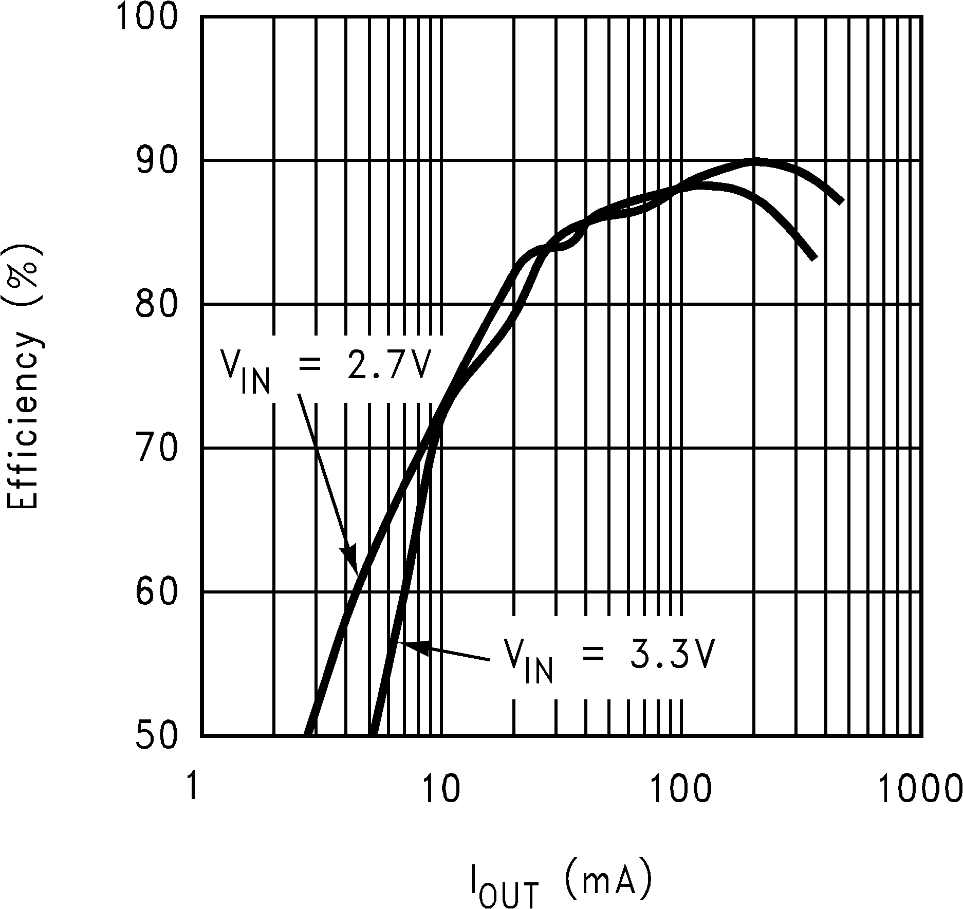
| VOUT = 8 V | fS = 1.25 MHz |
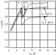
| 600 kHz | Switching |
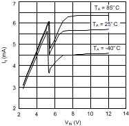
| 1.25 MHz | Switching |
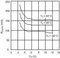 Figure 8. RDS(ON) vs VIN
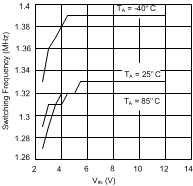 Figure 10. Switching Frequency vs VIN (1.25 MHz)
