SNVS217G May 2004 – September 2015 LM2731
PRODUCTION DATA.
- 1 Features
- 2 Applications
- 3 Description
- 4 Revision History
- 5 Pin Configuration and Functions
- 6 Specifications
- 7 Detailed Description
-
8 Application and Implementation
- 8.1 Application Information
- 8.2
Typical Application
- 8.2.1 Design Requirements
- 8.2.2
Detailed Design Procedure
- 8.2.2.1 Selecting the External Capacitors
- 8.2.2.2 Selecting the Output Capacitor
- 8.2.2.3 Selecting the Input Capacitor
- 8.2.2.4 Feedforward Compensation
- 8.2.2.5 Selecting Diodes
- 8.2.2.6 Setting the Output Voltage
- 8.2.2.7 Switching Frequency
- 8.2.2.8 Duty Cycle
- 8.2.2.9 Inductance Value
- 8.2.2.10 Maximum Switch Current
- 8.2.2.11 Calculating Load Current
- 8.2.2.12 Design Parameters VSW and ISW
- 8.2.2.13 Inductor Suppliers
- 8.2.3 Application Curves
- 8.3 System Examples
- 9 Power Supply Recommendations
- 10Layout
- 11Device and Documentation Support
- 12Mechanical, Packaging, and Orderable Information
Package Options
Mechanical Data (Package|Pins)
- DBV|5
Thermal pad, mechanical data (Package|Pins)
Orderable Information
6 Specifications
6.1 Absolute Maximum Ratings(1)
| MIN | MAX | UNIT | ||
|---|---|---|---|---|
| Operating Junction Temperature | –40 | 125 | °C | |
| Lead Temperature (Soldering, 5 sec.) | 300 | °C | ||
| Power Dissipation(2) | Internally Limited | |||
| FB Pin Voltage | –0.4 | 6 | V | |
| SW Pin Voltage | –0.4 | 22 | V | |
| Input Supply Voltage | –0.4 | 14.5 | V | |
| SHDN Pin Voltage | –0.4 | VIN + 0.3 | V | |
| Storage Temperature, Tstg | –65 | 150 | °C | |
(1) Stresses beyond those listed under Absolute Maximum Ratings may cause permanent damage to the device. These are stress ratings only, which do not imply functional operation of the device at these or any other conditions beyond those indicated under Recommended Operating Conditions. Exposure to absolute-maximum-rated conditions for extended periods may affect device reliability.
(2) The maximum power dissipation which can be safely dissipated for any application is a function of the maximum junction temperature, TJ(MAX) = 125°C, the junction-to-ambient thermal resistance for the SOT-23 package, RθJA = 265°C/W, and the ambient temperature, TA. The maximum allowable power dissipation at any ambient temperature for designs using this device can be calculated using the formula:  . If power dissipation exceeds the maximum specified above, the internal thermal protection circuitry will protect the device by reducing the output voltage as required to maintain a safe junction temperature.
 . If power dissipation exceeds the maximum specified above, the internal thermal protection circuitry will protect the device by reducing the output voltage as required to maintain a safe junction temperature.
6.2 ESD Ratings
| VALUE | UNIT | |||
|---|---|---|---|---|
| V(ESD) | Electrostatic discharge | Human body model (HBM), per ANSI/ESDA/JEDEC JS-001(1)(2) | ±2000 | V |
(1) JEDEC document JEP155 states that 500-V HBM allows safe manufacturing with a standard ESD control process.
(2) The human body model is a 100-pF capacitor discharged through a 1.5-kΩ resistor into each pin.
6.3 Recommended Operating Conditions
over operating free-air temperature range (unless otherwise noted)| MIN | NOM | MAX | UNIT | ||
|---|---|---|---|---|---|
| VIN | Input Supply Voltage | 2.7 | 14 | V | |
| Vsw | SW Pin Voltage | 3 | 20 | V | |
| Vshdn | Shutdown Supply Voltage(1) | 0 | VIN | V | |
| TJ | Junction Temperature Range | –40 | 125 | ºC | |
(1) This pin should not be allowed to float or be greater than VIN + 0.3 V.
6.4 Thermal Information
| THERMAL METRIC(1) | LM2731 | UNIT | |
|---|---|---|---|
| DBV (SOT-23) | |||
| 5 PINS | |||
| RθJA | Junction-to-ambient thermal resistance | 209.9 | °C/W |
| RθJC(top) | Junction-to-case (top) thermal resistance | 122 | °C/W |
| RθJB | Junction-to-board thermal resistance | 38.4 | °C/W |
| ψJT | Junction-to-top characterization parameter | 12.8 | °C/W |
| ψJB | Junction-to-board characterization parameter | 37.5 | °C/W |
| RθJC(bot) | Junction-to-case (bottom) thermal resistance | N/A | °C/W |
(1) For more information about traditional and new thermal metrics, see the Semiconductor and IC Package Thermal Metrics application report, SPRA953.
6.5 Electrical Characteristics
Limits are for TJ = 25°C. Unless otherwise specified: VIN = 5 V, VSHDN = 5 V, IL = 0 A.| PARAMETER | TEST CONDITIONS | MIN(1) | TYP(2) | MAX(1) | UNIT | ||
|---|---|---|---|---|---|---|---|
| VIN | Input Voltage | −40°C ≤ TJ ≤ 125°C | 2.7 | 14 | V | ||
| VOUT (MIN) | Minimum Output Voltage Under Load | RL = 43 Ω X Option(5) |
VIN = 2.7 V | 7 | V | ||
| −40°C ≤ TJ ≤ 125°C | 5.4 | ||||||
| VIN = 3.3 V | 10 | ||||||
| −40°C ≤ TJ ≤ 125°C | 8 | ||||||
| VIN = 5 V | 16 | ||||||
| RL = 43 Ω Y Option(5) |
VIN = 2.7 V | 7.5 | |||||
| −40°C ≤ TJ ≤ 125°C | 6 | ||||||
| VIN = 3.3 V | 11 | ||||||
| −40°C ≤ TJ ≤ 125°C | 8.75 | ||||||
| VIN = 5 V | 15 | ||||||
| RL = 15 Ω X Option(5) |
VIN = 2.7 V | 5 | |||||
| −40°C ≤ TJ ≤ 125°C | 3.75 | ||||||
| VIN = 3.3 V | 6.5 | ||||||
| −40°C ≤ TJ ≤ 125°C | 5 | ||||||
| VIN = 5 V | 10 | ||||||
| RL = 15 Ω Y Option(5) |
VIN = 2.7 V | 5 | |||||
| −40°C ≤ TJ ≤ 125°C | 4 | ||||||
| VIN = 3.3 V | 7 | ||||||
| −40°C ≤ TJ ≤ 125°C | 5.5 | ||||||
| VIN = 5 V | 10 | ||||||
| ISW | Switch Current Limit | See(3) | TJ = 25°C | 1.8 | 2 | A | |
| −40°C ≤ TJ ≤ 125°C | 1.4 | ||||||
| RDS(ON) | Switch ON-Resistance | ISW = 100 mA Vin = 5 V |
TJ = 25°C | 260 | 400 | mΩ | |
| −40°C ≤ TJ ≤ 125°C | 500 | ||||||
| ISW = 100 mA Vin = 3.3 V |
TJ = 25°C | 300 | 450 | ||||
| −40°C ≤ TJ ≤ 125°C | 550 | ||||||
| SHDNTH | Shutdown Threshold | Device ON | −40°C ≤ TJ ≤ 125°C | 1.5 | V | ||
| Device OFF | −40°C ≤ TJ ≤ 125°C | 0.5 | |||||
| ISHDN | Shutdown Pin Bias Current | VSHDN = 0 | 0 | µA | |||
| VSHDN = 5 V | TJ = 25°C | 0 | |||||
| −40°C ≤ TJ ≤ 125°C | 2 | ||||||
| VFB | Feedback Pin Reference Voltage | VIN = 3 V | TJ = 25°C | 1.230 | V | ||
| −40°C ≤ TJ ≤ 125°C | 1.205 | 1.255 | |||||
| IFB | Feedback Pin Bias Current | VFB = 1.23 V | TJ = 25°C | 60 | nA | ||
| −40°C ≤ TJ ≤ 125°C | 500 | ||||||
| IQ | Quiescent Current | VSHDN = 5 V, Switching "X" | TJ = 25°C | 2 | mA | ||
| −40°C ≤ TJ ≤ 125°C | 3 | ||||||
| VSHDN = 5 V, Switching "Y" | TJ = 25°C | 1 | |||||
| −40°C ≤ TJ ≤ 125°C | 2 | ||||||
| VSHDN = 5 V, Not Switching | TJ = 25°C | 400 | µA | ||||
| −40°C ≤ TJ ≤ 125°C | 500 | ||||||
| VSHDN = 0 | 0.024 | 1 | |||||
| ΔVFB/ΔVIN | FB Voltage Line Regulation | 2.7 V ≤ VIN ≤ 14 V | 0.02 | %/V | |||
| FSW | Switching Frequency(4) | “X” Option | TJ = 25°C | 1.6 | MHz | ||
| −40°C ≤ TJ ≤ 125°C | 1 | 1.85 | |||||
| “Y” Option | TJ = 25°C | 0.6 | |||||
| −40°C ≤ TJ ≤ 125°C | 0.4 | 0.8 | |||||
| DMAX | Maximum Duty Cycle(4) | “X” Option | TJ = 25°C | 86% | |||
| −40°C ≤ TJ ≤ 125°C | 78% | ||||||
| “Y” Option | TJ = 25°C | 93% | |||||
| −40°C ≤ TJ ≤ 125°C | 88% | ||||||
| IL | Switch Leakage | Not Switching VSW = 5 V | 1 | µA | |||
(1) Limits are ensured by testing, statistical correlation, or design.
(2) Typical values are derived from the mean value of a large quantity of samples tested during characterization and represent the most likely expected value of the parameter at room temperature.
(3) Switch current limit is dependent on duty cycle (see Typical Characteristics).
(4) Specified limits are the same for Vin = 3.3 V input.
(5) L = 10 µH, COUT = 4.7 µF, duty cycle = maximum
6.6 Typical Characteristics
Unless otherwise specified: VIN = 5 V, SHDN pin tied to VIN. Figure 1. Iq VIN (Active) vs Temperature - X Option
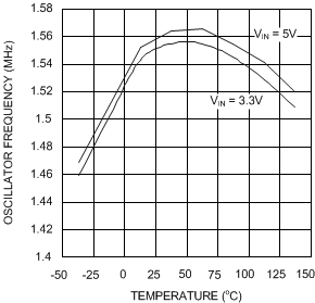 Figure 3. Oscillator Frequency vs Temperature - X Option
 Figure 5. Maximum Duty Cycle vs Temperature - X Option
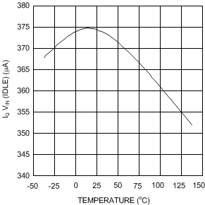 Figure 7. Iq VIN (Idle) vs Temperature
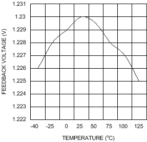 Figure 9. Feedback Voltage vs Temperature
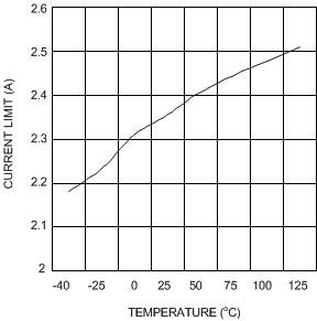 Figure 11. Current Limit vs Temperature

| VIN = 2.7 V | VOUT = 5 V |
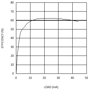
| VIN = 2.7 V | VOUT = 12 V |

| VIN = 5 V | VOUT = 18 V |

| VIN = 3.3 V | VOUT = 5 V |

| VIN = 2.7 V | VOUT = 12 V |

| VIN = 5 V | VOUT = 12 V | |

 Figure 4. Oscillator Frequency vs Temperature - Y Option
 Figure 6. Maximum Duty Cycle vs Temperature - Y Option
 Figure 8. Feedback Bias Current vs Temperature
 Figure 10. RDS(ON) vs Temperature
 Figure 12. RDS(ON) vs VIN

| VIN = 4.2 V | VOUT = 5 V |
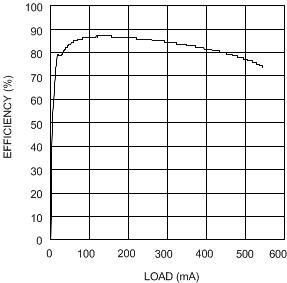
| VIN = 5 V | VOUT = 12 V |
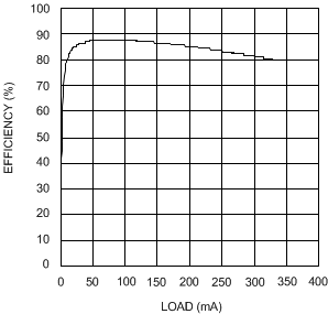
| VIN = 2.7 V | VOUT = 5 V |
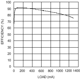
| VIN = 4.2 V | VOUT = 5 V | |

| VIN = 3.3 V | VOUT = 12 V |