SNVS485I June 2007 – September 2018 LM2735
PRODUCTION DATA.
- 1 Features
- 2 Applications
- 3 Description
- 4 Revision History
- 5 Pin Configuration and Functions
- 6 Specifications
- 7 Detailed Description
-
8 Application and Implementation
- 8.1 Application Information
- 8.2
Typical Applications
- 8.2.1 LM2735X SOT-23 Design Example 1
- 8.2.2 LM2735Y SOT-23 Design Example 2
- 8.2.3 LM2735X WSON Design Example 3
- 8.2.4 LM2735Y WSON Design Example 4
- 8.2.5 LM2735Y MSOP-PowerPAD Design Example 5
- 8.2.6 LM2735X SOT-23 Design Example 6
- 8.2.7 LM2735Y SOT-23 Design Example 7
- 8.2.8 LM2735X SOT-23 Design Example 8
- 8.2.9 LM2735Y SOT-23 Design Example 9
- 8.2.10 LM2735X WSON Design Example 10
- 8.2.11 LM2735Y WSON Design Example 11
- 8.2.12 LM2735X WSON SEPIC Design Example 12
- 8.2.13 LM2735Y MSOP-PowerPAD SEPIC Design Example 13
- 8.2.14 LM2735X SOT-23 LED Design Example 14
- 8.2.15 LM2735Y WSON FlyBack Design Example 15
- 8.2.16 LM2735X SOT-23 LED Design Example 16 VRAIL > 5.5 V Application
- 8.2.17 LM2735X SOT-23 LED Design Example 17 Two-Input Voltage Rail Application
- 8.2.18 SEPIC Converter
- 9 Power Supply Recommendations
- 10Layout
- 11Device and Documentation Support
- 12Mechanical, Packaging, and Orderable Information
Package Options
Mechanical Data (Package|Pins)
Thermal pad, mechanical data (Package|Pins)
- DGN|8
Orderable Information
6.6 Typical Characteristics
 Figure 1. Current Limit vs Temperature
  Figure 3. Oscillator Frequency vs Temperature - "X"
  Figure 5. Typical Maximum Output Current vs VIN
VO = 20 V
Figure 7. LM2735X Efficiency vs Load Current 
VO = 12 V
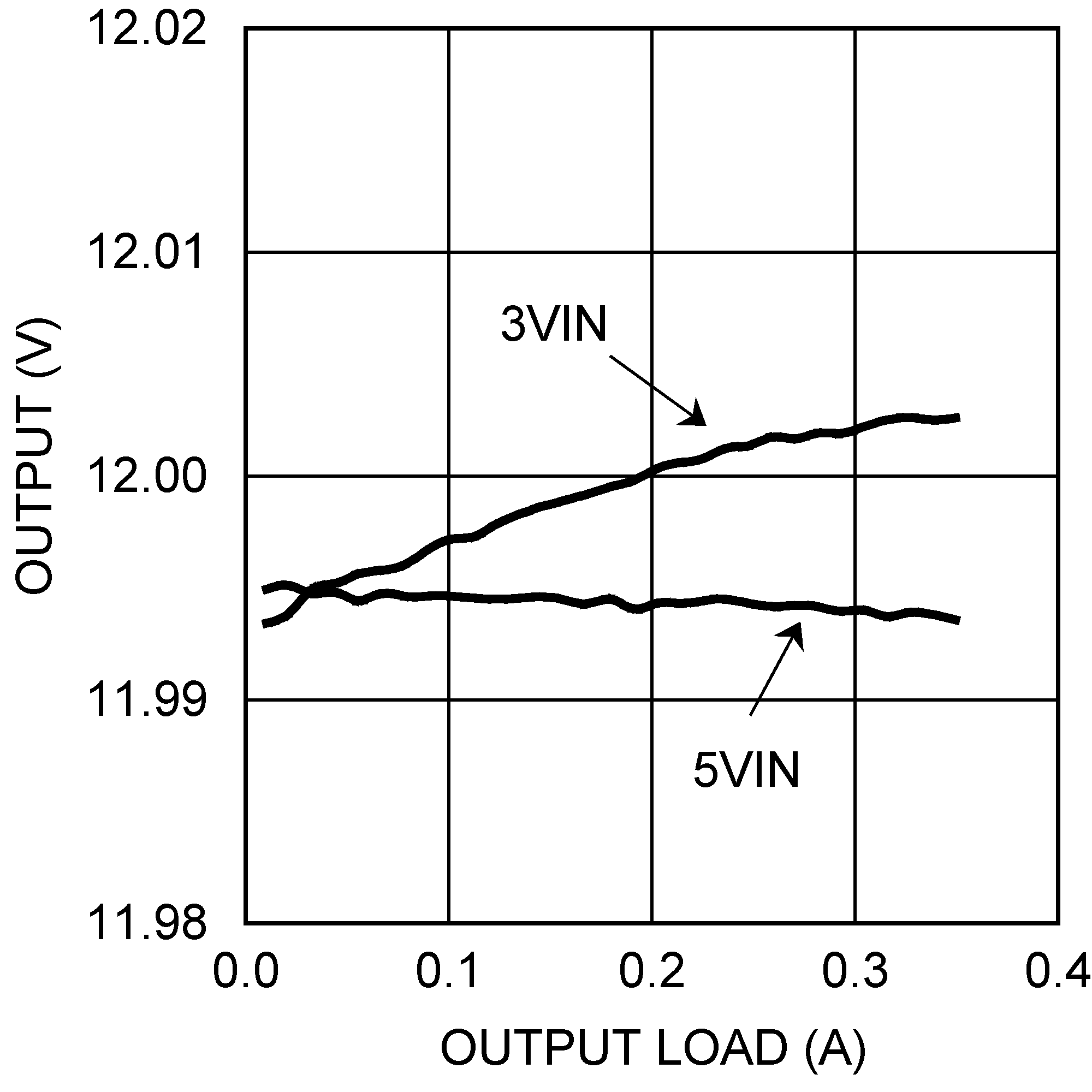
Figure 9. LM2735X Efficiency vs Load Current  Figure 11. Output Voltage Load Regulation
  Figure 2. FB Pin Voltage vs Temperature
  Figure 4. Oscillator Frequency vs Temperature - "Y"
  Figure 6. RDSON vs Temperature
VO = 20 V
Figure 8. LM2735Y Efficiency vs Load Current 
VO = 12 V
Figure 10. LM2735Y Efficiency vs Load Current  Figure 12. Output Voltage Line Regulation