SNVS556C April   2008  – January 2016 LM2738

PRODUCTION DATA.  

  1. Features
  2. Applications
  3. Description
  4. Revision History
  5. Pin Configuration and Functions
  6. Specifications
    1. 6.1 Absolute Maximum Ratings
    2. 6.2 ESD Ratings
    3. 6.3 Recommended Operating Conditions
    4. 6.4 Thermal Information
    5. 6.5 Electrical Characteristics
    6. 6.6 Typical Characteristics
  7. Detailed Description
    1. 7.1 Overview
    2. 7.2 Functional Block Diagram
    3. 7.3 Feature Description
      1. 7.3.1 Boost Function
      2. 7.3.2 Soft-Start
      3. 7.3.3 Output Overvoltage Protection
      4. 7.3.4 Undervoltage Lockout
      5. 7.3.5 Current Limit
      6. 7.3.6 Thermal Shutdown
    4. 7.4 Device Functional Modes
      1. 7.4.1 Enable Pin and Shutdown Mode
  8. Application and Implementation
    1. 8.1 Application Information
    2. 8.2 Typical Applications
      1. 8.2.1  LM2738X Circuit Example 1
        1. 8.2.1.1 Design Requirements
        2. 8.2.1.2 Detailed Design Procedure
          1. 8.2.1.2.1 Inductor Selection
          2. 8.2.1.2.2 Input Capacitor
          3. 8.2.1.2.3 Output Capacitor
          4. 8.2.1.2.4 Catch Diode
          5. 8.2.1.2.5 Output Voltage
          6. 8.2.1.2.6 Calculating Efficiency and Junction Temperature
        3. 8.2.1.3 Application Curve
      2. 8.2.2  LM2738X Circuit Example 2
        1. 8.2.2.1 Detailed Design Procedure
        2. 8.2.2.2 Application Curve
      3. 8.2.3  LM2738X Circuit Example 3
        1. 8.2.3.1 Detailed Design Procedure
        2. 8.2.3.2 Application Curve
      4. 8.2.4  LM2738X Circuit Example 4
        1. 8.2.4.1 Detailed Design Procedure
      5. 8.2.5  LM2738X Circuit Example 5
        1. 8.2.5.1 Detailed Design Procedure
      6. 8.2.6  LM2738Y Circuit Example 6
        1. 8.2.6.1 Detailed Design Procedure
        2. 8.2.6.2 Application Curve
      7. 8.2.7  LM2738Y Circuit Example 7
        1. 8.2.7.1 Detailed Design Procedure
        2. 8.2.7.2 Application Curve
      8. 8.2.8  LM2738Y Circuit Example 8
        1. 8.2.8.1 Detailed Design Procedure
        2. 8.2.8.2 Application Curve
      9. 8.2.9  LM2738Y Circuit Example 9
        1. 8.2.9.1 Detailed Design Procedure
        2. 8.2.9.2 Application Curve
      10. 8.2.10 LM2738Y Circuit Example 10
        1. 8.2.10.1 Detailed Design Procedure
  9. Power Supply Recommendations
  10. 10Layout
    1. 10.1 Layout Guidelines
      1. 10.1.1 WSON Package
    2. 10.2 Layout Example
    3. 10.3 Thermal Considerations
      1. 10.3.1 Silicon Junction Temperature Determination Methods
        1. 10.3.1.1 Method 1
        2. 10.3.1.2 Method 2
  11. 11Device and Documentation Support
    1. 11.1 Device Support
      1. 11.1.1 Third-Party Products Disclaimer
    2. 11.2 Documentation Support
      1. 11.2.1 Related Documentation
    3. 11.3 Community Resources
    4. 11.4 Trademarks
    5. 11.5 Electrostatic Discharge Caution
    6. 11.6 Glossary
  12. 12Mechanical, Packaging, and Orderable Information

Package Options

Mechanical Data (Package|Pins)
Thermal pad, mechanical data (Package|Pins)
Orderable Information

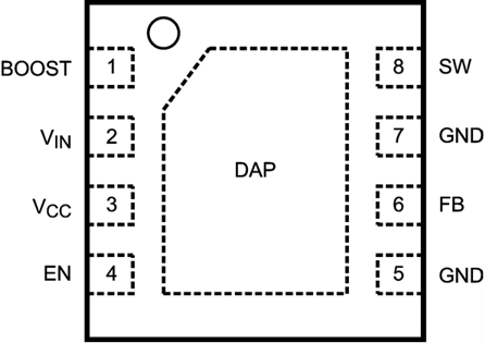
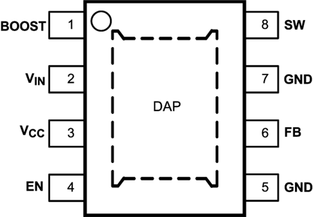
5 Pin Configuration and Functions

NGQ Package
8-Pin WSON With Exposed Thermal Pad
Top View
LM2738 30049161.png
DGN Package
8-Pin MSOP-PowerPAD
Top View
LM2738 30049163.png

Pin Functions

PIN TYPE(1) DESCRIPTION
NO. NAME
1 BOOST I Boost voltage that drives the internal NMOS control switch. A bootstrap capacitor is connected between the BOOST and SW pins.
2 VIN PWR Supply voltage for output power stage. Connect a bypass capacitor to this pin. Must tie pins 2 and 3 together at package.
3 VCC I Input supply voltage of the device. Connect a bypass capacitor to this pin. Must tie pins 2 and 3 together at the package.
4 EN I Enable control input. Logic high enables operation. Do not allow this pin to float or be greater than VIN + 0.3 V.
5, 7 GND PWR Signal and power ground pins. Place the bottom resistor of the feedback network as close as possible to these pins.
6 FB I Feedback pin. Connect FB to the external resistor divider to set output voltage.
8 SW O Output switch. Connects to the inductor, catch diode, and bootstrap capacitor.
DAP GND Signal and power ground. Must be connected to GND on the PCB.
(1) I = Input, O = Output, and PWR = Power