6 Specifications
6.1 Absolute Maximum Ratings
over operating free-air temperature range (unless otherwise noted) (1)(2)
|
MIN |
MAX |
UNIT |
| VIN, VCC |
–0.5 |
24 |
V |
| SW voltage |
–0.5 |
24 |
V |
| Boost voltage |
–0.5 |
30 |
V |
| Boost to SW voltage |
–0.5 |
6 |
V |
| FB voltage |
–0.5 |
3 |
V |
| EN voltage |
–0.5 |
VIN + 0.3 |
V |
| Junction temperature |
|
150 |
°C |
| Soldering information |
Infrared and convection reflow (15 s) |
|
220 |
°C |
| Wave soldering lead temperature (10 s) |
|
260 |
°C |
| Storage temperature, Tstg |
–65 |
150 |
°C |
(1) Stresses beyond those listed under Absolute Maximum Ratings may cause permanent damage to the device. These are stress ratings only, which do not imply functional operation of the device at these or any other conditions beyond those indicated under Recommended Operating Conditions. Exposure to absolute-maximum-rated conditions for extended periods may affect device reliability.
(2) If Military or Aerospace specified devices are required, contact the Texas Instruments Sales Office or Distributors for availability and specifications.
6.2 ESD Ratings
|
VALUE |
UNIT |
| V(ESD) |
Electrostatic discharge |
Human-body model (HBM), per ANSI/ESDA/JEDEC JS-001(1)(2) |
±2000 |
V |
(1) JEDEC document JEP155 states that 500-V HBM allows safe manufacturing with a standard ESD control process.
(2) Human body model, 1.5 kΩ in series with 100 pF.
6.3 Recommended Operating Conditions
over operating free-air temperature range (unless otherwise noted)
|
MIN |
MAX |
UNIT |
| VIN, VCC |
3 |
20 |
V |
| SW voltage |
–0.5 |
20 |
V |
| Boost voltage |
–0.5 |
25.5 |
V |
| Boost to SW voltage |
2.5 |
5.5 |
V |
| Junction temperature |
−40 |
125 |
°C |
| Thermal shutdown |
|
165 |
°C |
6.4 Thermal Information
| THERMAL METRIC(1) |
LM2738 |
UNIT |
| NGQ (WSON) |
DGN (MSOP PowerPAD) |
| 8 PINS |
8 PINS |
| RθJA |
Junction-to-ambient thermal resistance (2) |
45.9 |
50.3 |
°C/W |
| RθJC(top) |
Junction-to-case (top) thermal resistance |
44.6 |
54.2 |
°C/W |
| RθJB |
Junction-to-board thermal resistance |
13.2 |
31.4 |
°C/W |
| ψJT |
Junction-to-top characterization parameter |
0.5 |
4.8 |
°C/W |
| ψJB |
Junction-to-board characterization parameter |
13.2 |
31.2 |
°C/W |
| RθJC(bot) |
Junction-to-case (bottom) thermal resistance |
5.8 |
4 |
°C/W |
(1) For more information about traditional and new thermal metrics, see the
Semiconductor and device Package Thermal Metrics application report,
SPRA953.
(2) Typical thermal shutdown occurs if the junction temperature exceeds 165°C. The maximum power dissipation is a function of TJ(MAX) , RθJA and TA . The maximum allowable power dissipation at any ambient temperature is PD = (TJ(MAX) – TA) / RθJA. All numbers apply for packages soldered directly onto a 3 inches × 3 inches PC board with 2 oz. copper on 4 layers in still air in accordance to JEDEC standards. Thermal resistance varies greatly with layout, copper thickness, number of layers in PCB, power distribution, number of thermal vias, board size, ambient temperature, and air flow.
6.5 Electrical Characteristics
All typical limits apply over TJ = 25°C, and all maximum and minimum limits apply over the full operating temperature range (TJ = –40°C to +125°C). VIN = 12 V, VBOOST – VSW = 5 V unless otherwise specified. Data sheet minimum and maximum specification limits are ensured by design, test, or statistical analysis.
| PARAMETER |
TEST CONDITIONS |
MIN(1) |
TYP(2) |
MAX(1) |
UNIT |
| VFB |
Feedback voltage |
|
0.784 |
0.800 |
0.816 |
V |
| ΔVFB/ΔVIN |
Feedback voltage line regulation |
VIN = 3 V to 20 V |
|
0.02 |
|
%/V |
| IFB |
Feedback input bias current |
Sink or source |
|
0.1 |
100 |
nA |
| UVLO |
Undervoltage lockout |
VIN Rising |
|
2.7 |
2.9 |
V |
| Undervoltage lockout |
VIN Falling |
2 |
2.3 |
|
| UVLO hysteresis |
|
|
0.4 |
|
| FSW |
Switching frequency |
LM2738X |
1.28 |
1.6 |
1.92 |
MHz |
| LM2738Y |
0.364 |
0.55 |
0.676 |
| DMAX |
Maximum duty cycle |
LM2738X , Load = 150 mA |
|
92% |
|
|
| LM2738Y, Load = 150 mA |
|
95% |
|
| DMIN |
Minimum duty cycle |
LM2738X |
|
7.5% |
|
|
| LM2738Y |
|
2% |
|
| RDS(ON) |
Switch ON resistance |
VBOOST – VSW = 3 V, Load = 400 mA |
|
250 |
500 |
mΩ |
| ICL |
Switch current limit |
VBOOST – VSW = 3 V, VIN = 3 V |
2 |
2.9 |
|
A |
| IQ |
Quiescent current |
Switching |
|
1.9 |
3 |
mA |
| Non-Switching |
|
1.9 |
|
mA |
| Quiescent current (shutdown) |
VEN = 0 V |
|
400 |
|
nA |
| IBOOST |
Boost pin current |
LM2738X (27% Duty Cycle) |
|
4.5 |
|
mA |
| LM2738Y (27% Duty Cycle) |
|
2.5 |
|
| VEN_TH |
Shutdown threshold voltage |
VEN Falling |
|
|
0.4 |
V |
| Enable threshold voltage |
VEN Rising |
1.4 |
|
|
| IEN |
Enable pin current |
Sink / Source |
|
10 |
|
nA |
| ISW |
Switch leakage |
VIN = 20 V |
|
100 |
|
nA |
(1) Ensured to average outgoing quality level (AOQL).
(2) Typicals represent the most likely parametric norm.
6.6 Typical Characteristics
All curves taken at VIN = 12 V, VBOOST – VSW = 5 V, and TA = 25°C, unless specified otherwise.
 Figure 1. Efficiency vs Load Current – X Version
 Figure 3. Efficiency vs Load Current – X Version
 Figure 5. Efficiency vs Load Current – X Version
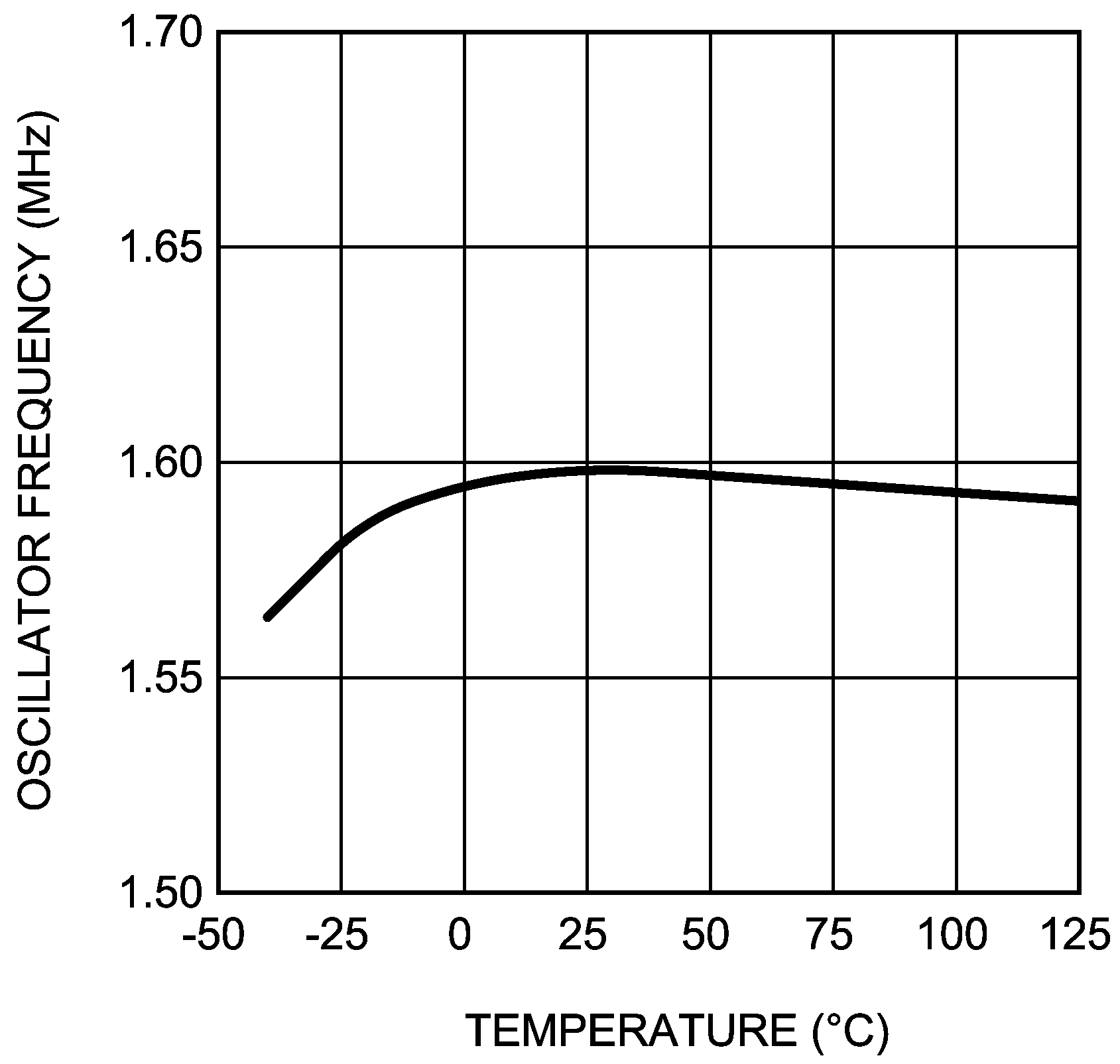
 Figure 7. Oscillator Frequency vs Temperature – X Version
 Figure 9. Current Limit vs Temperature
 Figure 11. VFB vs Temperature

| VOUT = 1.5 V |
IOUT = 750 mA |
|
Figure 13. Line Regulation – X Version

| VOUT = 3.3 V |
IOUT = 750 mA |
|
Figure 15. Line Regulation – X Version
 Figure 17. Load Regulation – X Version
 Figure 19. Load Regulation – X Version
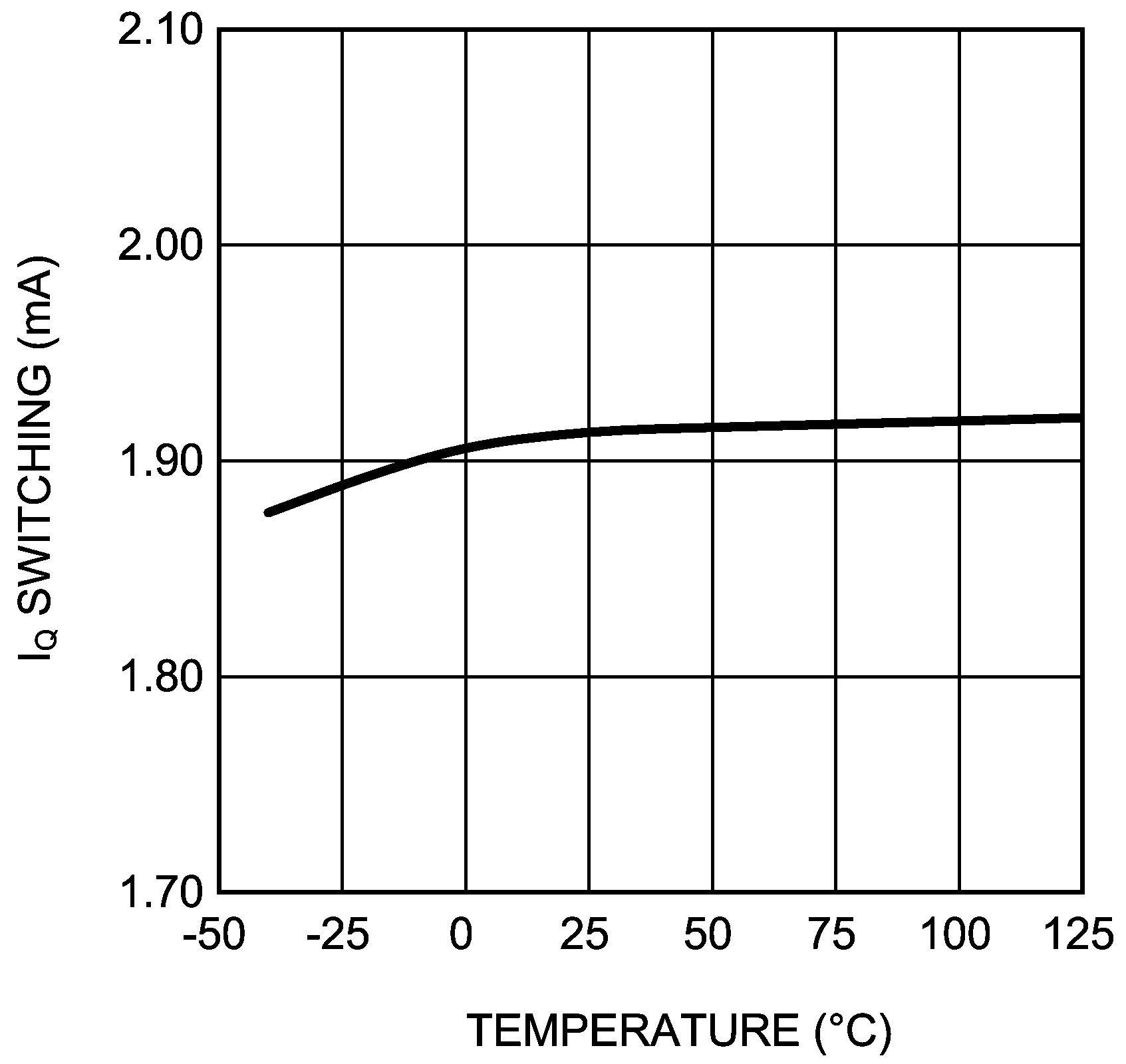
 Figure 21. IQ Switching vs Temperature

| VOUT = 3.3 V |
VIN = 12 V |
IOUT = 1.5 A |
Figure 23. Startup – X Version (Resistive Load)
 Figure 2. Efficiency vs Load Current – Y Version
 Figure 4. Efficiency vs Load Current – Y Version
 Figure 6. Efficiency vs Load Current – Y Version
 Figure 8. Oscillator Frequency vs Temperature – Y Version
 Figure 10. IQ Non-Switching vs Temperature
 Figure 12. RDSON vs Temperature

| VOUT = 1.5 V |
IOUT = 750 mA |
|
Figure 14. Line Regulation – Y Version

| VOUT = 3.3 V |
IOUT = 750 mA |
|
Figure 16. Line Regulation – Y Version
 Figure 18. Load Regulation – Y Version
 Figure 20. Load Regulation – Y Version
 Figure 22. Load Transient – X Version

| VOUT = 3.3 V |
VIN = 12 V |
IOUT = 1.5 A |
Figure 24. In-Rush Current – X Version (Resistive Load)


 Figure 7. Oscillator Frequency vs Temperature – X Version

 Figure 11. VFB vs Temperature


 Figure 21. IQ Switching vs Temperature


 Figure 8. Oscillator Frequency vs Temperature – Y Version

 Figure 12. RDSON vs Temperature


