SNVS276I April 2004 – February 2019 LM2743
PRODUCTION DATA.
- 1 Features
- 2 Applications
- 3 Description
- 4 Revision History
- 5 Pin Configuration and Functions
- 6 Specifications
- 7 Detailed Description
- 8 Application and Implementation
- 9 Power Supply Recommendations
- 10Layout
- 11Device and Documentation Support
- 12Mechanical, Packaging, and Orderable Information
Package Options
Mechanical Data (Package|Pins)
- PW|14
Thermal pad, mechanical data (Package|Pins)
Orderable Information
8.2.1.2.8 Control Loop Compensation
The LM2743 uses voltage-mode (‘VM’) PWM control to correct changes in output voltage due to line and load transients. One of the attractive advantages of voltage mode control is its relative immunity to noise and layout. However VM requires careful small signal compensation of the control loop for achieving high bandwidth and good phase margin.
The control loop is comprised of two parts. The first is the power stage, which consists of the duty cycle modulator, output inductor, output capacitor, and load. The second part is the error amplifier, which for the LM2743 is a 9-MHz op-amp used in the classic inverting configuration. Figure 32 shows the regulator and control loop components.
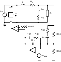 Figure 32. Power Stage and Error Amplifier
 One popular method for selecting the compensation components is to create Bode plots of gain and phase for the power stage and error amplifier. Combined, they make the overall bandwidth and phase margin of the regulator easy to see. Software tools such as Excel, MathCAD, and Matlab are useful for showing how changes in compensation or the power stage affect system gain and phase.
The power stage modulator provides a DC gain ADC that is equal to the input voltage divided by the peak-to-peak value of the PWM ramp. This ramp is 1.0VP-P for the LM2743. The inductor and output capacitor create a double pole at frequency fDP, and the capacitor ESR and capacitance create a single zero at frequency fESR. For this example, with VIN = 3.3 V, these quantities are:


In the equation for fDP, the variable RL is the power stage resistance, and represents the inductor DCR plus the on resistance of the top power MOSFET. RO is the output voltage divided by output current. The power stage transfer function GPS is given by the following equation, and Figure 34 shows Bode plots of the phase and gain in this example.

where
- a = LCO(RO + RC)
- b = L + CO(RORL + RORC + RCRL)
- c = RO + RL
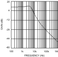 Figure 33. Gain vs Frequency
 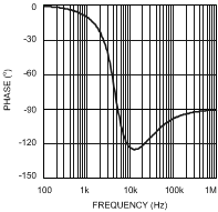 Figure 34. Power Stage Gain and Phase
 The double pole at 4.5 kHz causes the phase to drop to approximately -130° at around 10 kHz. The ESR zero, at 20.3 kHz, provides a +90° boost that prevents the phase from dropping to -180º. If this loop were left uncompensated, the bandwidth would be approximately 10 kHz and the phase margin 53°. In theory, the loop would be stable, but would suffer from poor DC regulation (due to the low DC gain) and would be slow to respond to load transients (due to the low bandwidth.) In practice, the loop could easily become unstable due to tolerances in the output inductor, capacitor, or changes in output current, or input voltage. Therefore, the loop is compensated using the error amplifier and a few passive components.
For this example, a Type III, or three-pole-two-zero approach gives optimal bandwidth and phase.
In most voltage mode compensation schemes, including Type III, a single pole is placed at the origin to boost DC gain as high as possible. Two zeroes fZ1 and fZ2 are placed at the double pole frequency to cancel the double pole phase lag. Then, a pole, fP1 is placed at the frequency of the ESR zero. A final pole fP2 is placed at one-half of the switching frequency. The gain of the error amplifier transfer function is selected to give the best bandwidth possible without violating the Nyquist stability criteria. In practice, a good crossover point is one-fifth of the switching frequency, or 60 kHz for this example. The generic equation for the error amplifier transfer function is:

In this equation, the variable AEA is a ratio of the values of the capacitance and resistance of the compensation components, arranged as shown in Figure 32. AEA is selected to provide the desired bandwidth. A starting value of 80,000 for AEA should give a conservative bandwidth. Increasing the value will increase the bandwidth, but will also decrease phase margin. Designs with 45° to 60° are usually best because they represent a good trade-off between bandwidth and phase margin. In general, phase margin is lowest and gain highest (worst-case) for maximum input voltage and minimum output current. One method to select AEA is to use an iterative process beginning with these worst-case conditions.
- Increase AEA
- Check overall bandwidth and phase margin
- Change VIN to minimum and recheck overall bandwidth and phase margin
- Change IO to maximum and recheck overall bandwidth and phase margin
The process ends when the both bandwidth and the phase margin are sufficiently high. For this example input voltage can vary from 3.0 to 3.6 V and output current can vary from 0 to 4 A, and after a few iterations a moderate gain factor of 101 dB is used.
The error amplifier of the LM2743 has a unity-gain bandwidth of 9 MHz. In order to model the effect of this limitation, the open-loop gain can be calculated as:

The new error amplifier transfer function that takes into account unity-gain bandwidth is:

The gain and phase of the error amplifier are shown in Figure 36.
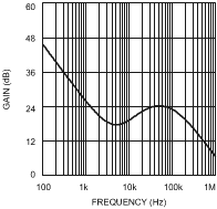 Figure 35. Gain vs Frequency
 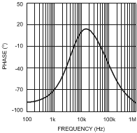 Figure 36. Error Amplifier Gain and Phase
 In VM regulators, the top feedback resistor RFB2 forms a part of the compensation. Setting RFB2 to 10 kΩ, ±1% usually gives values for the other compensation resistors and capacitors that fall within a reasonable range. (Capacitances > 1 pF, resistances < 1 MΩ) CC1, CC2, CC3, RC1, and RC2 are selected to provide the poles and zeroes at the desired frequencies, using the following equations:


In practice, a good trade off between phase margin and bandwidth can be obtained by selecting the closest ±10% capacitor values above what are suggested for CC1 and CC2, the closest ±10% capacitor value below the suggestion for CC3, and the closest ±1% resistor values below the suggestions for RC1, RC2. Note that if the suggested value for RC2 is less than 100Ω, it should be replaced by a short circuit. Following this guideline, the compensation components will be:
CC1 = 27 pF ±10%
CC2 = 820 pF ±10%
CC3 = 2.7 nF ±10%
RC1 = 39.2 kΩ ±1%
RC2 = 2.55 kΩ ±1%
The transfer function of the compensation block can be derived by considering the compensation components as impedance blocks ZF and ZI around an inverting op-amp:


As with the generic equation, GEA-ACTUAL must be modified to take into account the limited bandwidth of the error amplifier. The result is:

The total control loop transfer function H is equal to the power stage transfer function multiplied by the error amplifier transfer function.
The bandwidth and phase margin can be read graphically from Bode plots of HEA are shown in Figure 38.
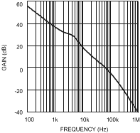 Figure 37. Gain vs Frequency
 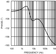 Figure 38. Overall Loop Gain and Phase
 The bandwidth of this example circuit is 59 kHz, with a phase margin of 60°.