SNVS353F February 2005 – September 2016 LM2753
PRODUCTION DATA.
- 1 Features
- 2 Applications
- 3 Description
- 4 Revision History
- 5 Pin Configuration and Functions
- 6 Specifications
- 7 Detailed Description
- 8 Application and Implementation
- 9 Power Supply Recommendations
- 10Layout
- 11Device and Documentation Support
- 12Mechanical, Packaging, and Orderable Information
Package Options
Mechanical Data (Package|Pins)
- DSC|10
Thermal pad, mechanical data (Package|Pins)
- DSC|10
Orderable Information
8 Application and Implementation
NOTE
Information in the following applications sections is not part of the TI component specification, and TI does not warrant its accuracy or completeness. TI’s customers are responsible for determining suitability of components for their purposes. Customers should validate and test their design implementation to confirm system functionality.
8.1 Application Information
The LM2753 can be used to drive a flash LED with a pulsed current of up to 400 mA or a continuous current of up to 200 mA over a wide input voltage range. As well as powering flash LEDs, the LM2753 device is suitable for driving other devices with power requirements up to 200 mA. White LEDs can also be connected to this device to back light a cellular phone keypad and display. The LED brightness can be controlled by applying a PWM signal to the enable pin (EN) during torch mode, or to the FLASH pin during flash mode (see PWM Brightness Control Procedures).
8.2 Typical Application
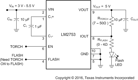 Figure 3. LM2753 Typical Application
8.2.1 Design Requirements
For typical switched-capacitor applications, use the parameters listed in Table 2.
Table 2. Design Parameters
| DESIGN PARAMETER | EXAMPLE VALUE |
|---|---|
| Minimum input voltage | 3 V |
| Typical output voltage | 5 V |
| Output current | 250 mA |
8.2.2 Detailed Design Procedure
8.2.2.1 Capacitors
The LM2753 requires three external capacitors for proper operation. TI recommends surface-mount multi-layer ceramic capacitors. These capacitors are small, inexpensive and have very low equivalent series resistance (ESR) ( ≤ 15 mΩ typical). Tantalum capacitors, OS-CON capacitors, and aluminum electrolytic capacitors are generally not recommended for use with the LM2753 due to their high ESR, as compared to ceramic capacitors.
For most applications, ceramic capacitors with X7R or X5R temperature characteristic are preferred for use with the LM2753. These capacitors have tight capacitance tolerance (as good as ±10%), hold their value over temperature (X7R: ±15% over −55°C to +125°C; X5R: ±15% over −55°C to +85°C), and typically have little voltage coefficient when compared to other types of capacitors. However, selecting a capacitor with a voltage rating much higher than the voltage it will be subjected to ensures that the capacitance stays closer to the nominal value of the capacitor. Capacitors with Y5V or Z5U temperature characteristic are generally not recommended for use with the LM2753. Capacitors with these temperature characteristics typically have wide capacitance tolerance (+80%, −20%), vary significantly over temperature (Y5V: 22%, −82% over −30°C to +85°C range; Z5U: 22%, −56% over 10°C to 85°C range), and have poor voltage coefficients. Under some conditions, a nominal 1-µF Y5V or Z5U capacitor could have a capacitance of only 0.1 µF. Such detrimental deviation is likely to cause Y5V and Z5U capacitors to fail to meet the minimum capacitance requirements of the LM2753. Table 3 lists suggested capacitor suppliers for the typical application circuit.
Table 3. Ceramic Capacitor Manufacturers
| MANUFACTURER | CONTACT |
|---|---|
| TDK | www.component.tdk.com |
| Murata | www.murata.com |
| Taiyo Yuden | www.t-yuden.com |
8.2.2.2 Power Dissipation
The power dissipation (PDISSIPATION) and junction temperature (TJ) can be approximated with Equation 3 and Equation 4. PIN is the product of the input current and input voltage, POUT is the power consumed by the load connected to the output, TA is the ambient temperature, and RθJA is the junction-to-ambient thermal resistance for the 10-pin WSON package.
where
- VIN is the input voltage to the LM2753
- VVOUT is the voltage at the output of the device
- IOUT is the total current supplied to the load(s) connected to both VOUT and IOUT
The junction temperature rating takes precedence over the ambient temperature rating. The LM2753 may be operated outside the ambient temperature rating, so long as the junction temperature of the device does not exceed the maximum operating rating of 120°C. The maximum ambient temperature rating must be derated in applications where high power dissipation and/or poor thermal resistance causes the junction temperature to exceed 120°C.
8.2.3 Application Curves
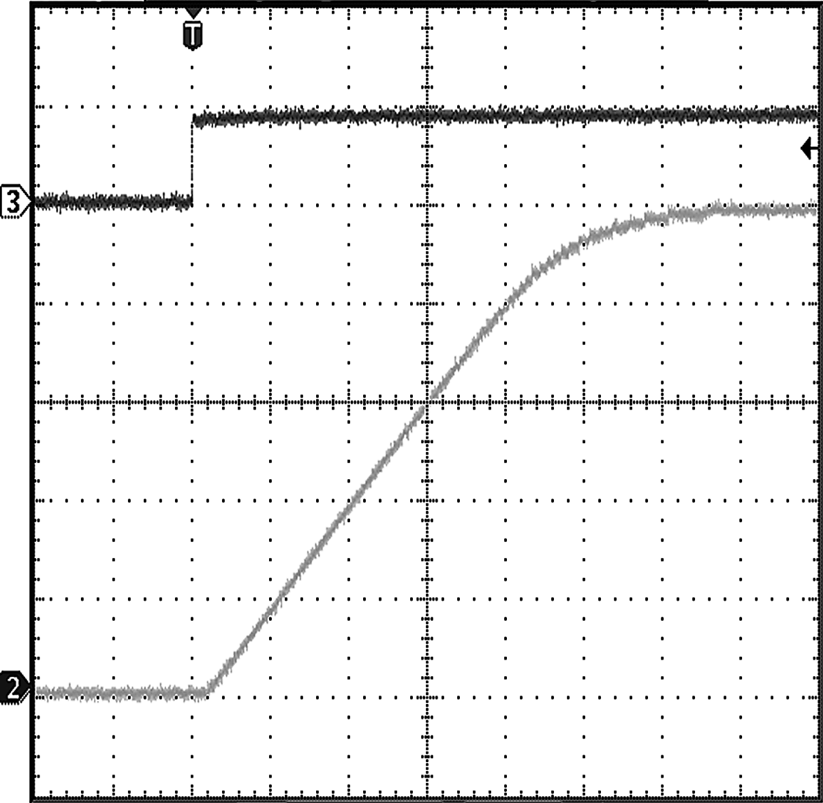
| Top:VEN; Scale: 2V/div | VIN = 3.6 V | |
| Bottom: VOUT; Scale: 1V/div | Load = 100 mA | |
| Time scale: 1000 µs/div | ||
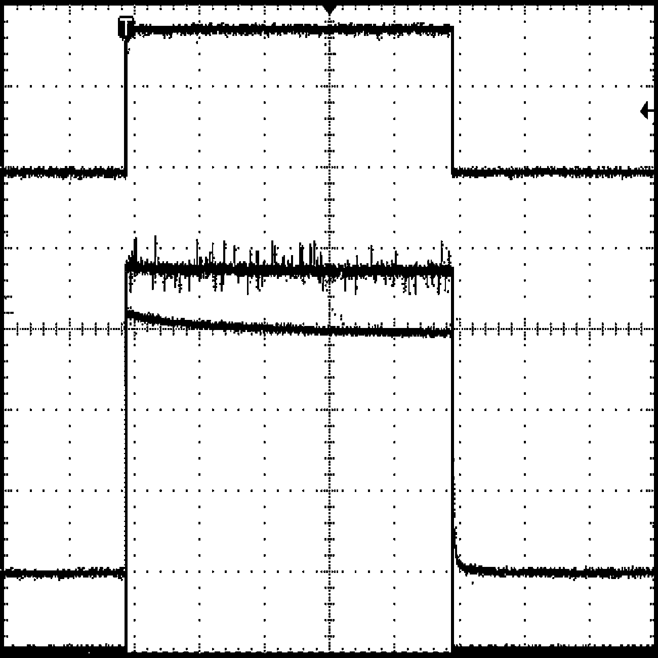
| Top:VFLASH; Scale: 1V/div | VIN = 3.6 V | |
| Bottom: VIOUT; Scale: 1V/div | Load = 10 mA to 400 mA Step | |
| Time scale: 100 ms/div | ||
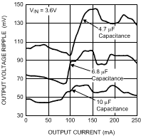
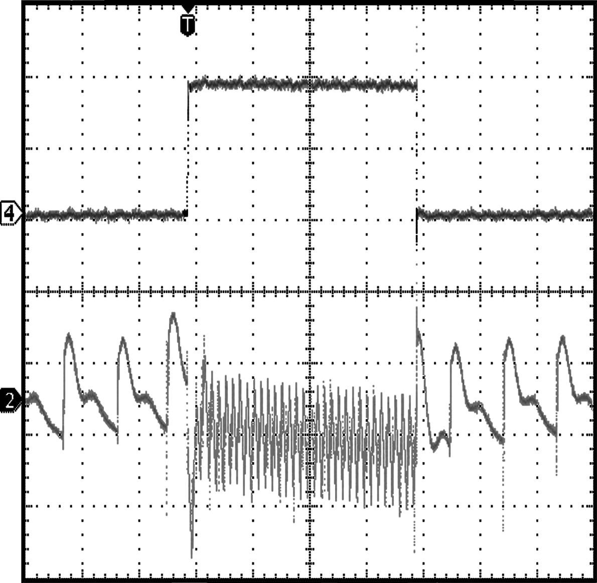
| Top: IVOUT; Scale: 100 mA/div | VIN = 3.6 V | ||
| Bottom: VOUT; Scale: 50 mV/div, AC Coupled | |||
| Time scale: 40 µs/div | |||
| Load = 10 mA to 20 mA Step | |||
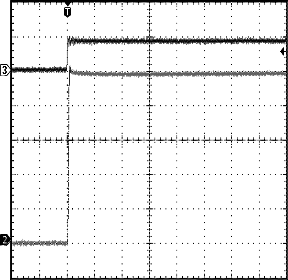
| Top:VFLASH; Scale: 2V/div | VIN = 3.6 V | |
| Bottom: VIOUT; Scale: 1V/div | No Load | |
| Time scale: 400 ns/div | ||
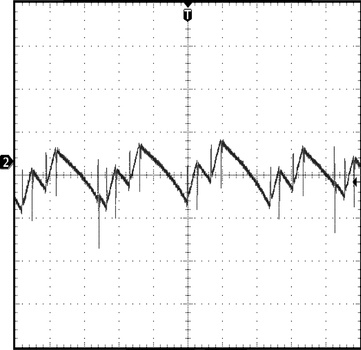
| VOUT; Scale: 50mV/Div, AC Coupled | VIN = 3.6 V | |
| Time scale: 2 µs/div | Load = 200 mA | |
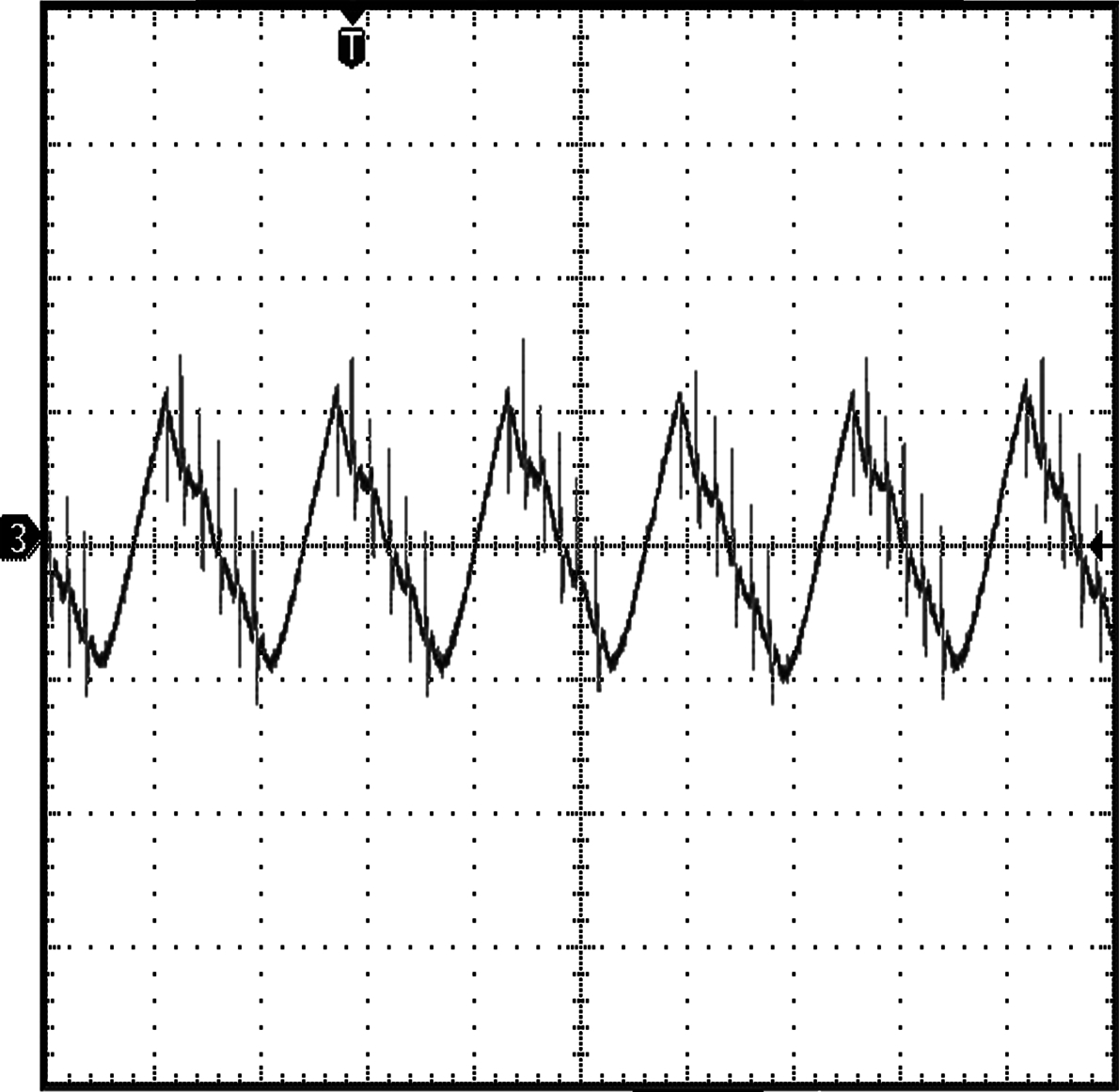
| VIN; Scale: 50mV/Div, AC Coupled | VIN = 3.6 V | |||
| Time scale: 4 µs/div | Load = 200 mA | |||