SNVS353F February   2005  – September 2016 LM2753

PRODUCTION DATA.  

  1. Features
  2. Applications
  3. Description
  4. Revision History
  5. Pin Configuration and Functions
  6. Specifications
    1. 6.1 Absolute Maximum Ratings
    2. 6.2 ESD Ratings
    3. 6.3 Recommended Operating Conditions
    4. 6.4 Thermal Information
    5. 6.5 Electrical Characteristics
    6. 6.6 Typical Characteristics
  7. Detailed Description
    1. 7.1 Overview
    2. 7.2 Functional Block Diagram
    3. 7.3 Feature Description
      1. 7.3.1 Soft Start
      2. 7.3.2 Flash LED Selection
      3. 7.3.3 PFM Regulation
      4. 7.3.4 Output Voltage Ripple
      5. 7.3.5 IOUT Pin
        1. 7.3.5.1 Setting Flash Current
        2. 7.3.5.2 Setting Torch Current
      6. 7.3.6 PWM Brightness Control Procedures
      7. 7.3.7 Multi-Level Switch Array
      8. 7.3.8 Thermal Protection
      9. 7.3.9 Power Efficiency
    4. 7.4 Device Functional Modes
      1. 7.4.1 Enable Mode
      2. 7.4.2 Flash Mode
  8. Application and Implementation
    1. 8.1 Application Information
    2. 8.2 Typical Application
      1. 8.2.1 Design Requirements
      2. 8.2.2 Detailed Design Procedure
        1. 8.2.2.1 Capacitors
        2. 8.2.2.2 Power Dissipation
      3. 8.2.3 Application Curves
  9. Power Supply Recommendations
  10. 10Layout
    1. 10.1 Layout Guidelines
    2. 10.2 Layout Example
  11. 11Device and Documentation Support
    1. 11.1 Device Support
      1. 11.1.1 Third-Party Products Disclaimer
    2. 11.2 Documentation Support
      1. 11.2.1 Related Documentation
    3. 11.3 Receiving Notification of Documentation Updates
    4. 11.4 Community Resources
    5. 11.5 Trademarks
    6. 11.6 Electrostatic Discharge Caution
    7. 11.7 Glossary
  12. 12Mechanical, Packaging, and Orderable Information

Package Options

Mechanical Data (Package|Pins)
Thermal pad, mechanical data (Package|Pins)
Orderable Information

10 Layout

10.1 Layout Guidelines

Place the output capacitor as close as possible to the output voltage and GND pins.

  • VIN input voltage pin must be bypassed to ground with a low-ESR bypass capacitor. Place the capacitor as close as possible to the VIN pin.
  • Place the charge pump flying capacitor close to the flying capacitor pins.

10.2 Layout Example
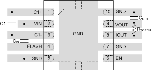
LM2753 layout_snvs353.gif Figure 12. LM2753 Layout