SNVS353F February 2005 – September 2016 LM2753
PRODUCTION DATA.
- 1 Features
- 2 Applications
- 3 Description
- 4 Revision History
- 5 Pin Configuration and Functions
- 6 Specifications
- 7 Detailed Description
- 8 Application and Implementation
- 9 Power Supply Recommendations
- 10Layout
- 11Device and Documentation Support
- 12Mechanical, Packaging, and Orderable Information
Package Options
Mechanical Data (Package|Pins)
- DSC|10
Thermal pad, mechanical data (Package|Pins)
- DSC|10
Orderable Information
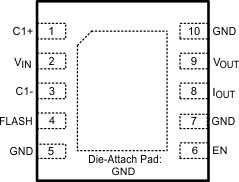
5 Pin Configuration and Functions
DSC Package
10-Pin WSON
Top View

Pin Descriptions
| PIN | TYPE | DESCRIPTION | |
|---|---|---|---|
| NUMBER | NAME | ||
| 1 | C1+ | O | Flying capacitor connection |
| 2 | VIN | I | Input voltage connection. Input voltage range: 3 V to 5.5 V |
| 3 | C1– | O | Flying capacitor connection |
| 4 | FLASH | I | Flash logic input pin. Logic HIGH = flash output on, logic low = flash output off. there is an internal pulldown of 300 kΩ between FLASH and GND. |
| 5 | GND | — | Connect to ground |
| 6 | EN | I | Enable pin. Logic HIGH = enable, Logic LOW = shutdown. There is an internal pulldown of 300 kΩ between EN and GND |
| 7 | GND | — | Connect to ground |
| 8 | IOUT | O | Flash output. ON/OFF control via FLASH pin |
| 9 | VOUT | O | 5-V regulated output |
| 10 | GND | — | Connect to ground |